Download
1 / 1
40 likes | 275 Views
Electroless 0,3 µm Au coating on thick Ni, deposited on Si. a b a – surface morphology and Auger profiling spectroscopy b – cross section morphology and EDS analysis. Vorobyova T. N. a , Reva O. V. b , Kobets A. V. a , Vrublevskaya O. N. a.

E N D
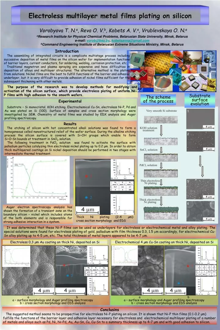
Electroless 0,3 µm Au coating on thick Ni, deposited on Si a b a – surface morphology and Auger profiling spectroscopy b – cross section morphology and EDS analysis Vorobyova T. N.a, Reva O. V.b, Kobets A. V.a, Vrublevskaya O. N.a aResearch Institute for Physical Chemical Problems, Belarusian State University, Minsk, Belarus e-mail: vorob@bsu.by, kobetsanna@gmail.com bCommand Engineering Institute of Belarusian Extreme Situations Ministry, Minsk, Belarus Introduction The assembling of integrated circuits is a complicate multistage process including successive deposition of metal films on the silicon wafer for implementation functions of barrier layers, current conductors, for soldering, welding, corrosion protection, etc. Traditional magnetron and plasma spraying are expensive and have difficulties in deposition of alloys and multilayer structures. The alternative method is the plating from solutions. Nickel films are the best to fulfill functions of the barrier and adhesive underlayer, but it is very difficult to provide adhesion of nickel films sufficient for the subsequent thickening with other metals. Electroless multilayer metal films plating on silicon The purpose of the research was to develop methods for modifying and activation of the silicon surface, which provide electroless plating of uniform Ni-P films with high adhesion to the smooth wafers. Substrate surface evolution The scheme of the process Experimental Substrate – Si monocristal. KOH etching. Electrochemical Cu-Sn, electroless Ni-P, Pd and Au was plated on Si (100). Surface of samples and cross section morphology were investigated by SEM. Chemistry of metal films was studied by EDXanalysis and Auger profiling spectroscopy. 1 1 Results The etching of silicon with hot concentrated alkali solutions was found to form a homogeneous celled nanostructured relief of the wafer surface. During the alkaline etching process the silicon surface is covered with Si–OH groups which enable to form Si–O–Sn bounds at treatment in SnCl2 solution. The following treatment in PdCl2 solution was found to activate the surface with palladium particles catalyzing thin electroless nickel plating up to 0.2 μm. In order to obtain thick multilayered coatings on Si nickel deposition should be performed in two stages with intermediate thermal treatment. 2 2 3 4 5 5 6 Auger electron spectroscopy analysis has shown the formation of a transient zone on the boundary silicon – nickel which includes atoms of the both elements and is responsible for strong adhesive interaction in a system. 6 Thick Ni plating (2-4 µm): cross section morphology and EDS It was determined that these Ni-P films can be used as underlayers for electroless or electrochemical metal and alloy plating. The special solutions were found for electroless plating of gold, palladium with film thickness 0.3, 1.5 m accordingly, for electrochemical Cu-Sn alloy plating up to 4-5 m, etc. The total thickness of metal layers appeared to be 4-7 m. Electrochemical 4 µm Cu-Sn coating on thick Ni, deposited on Si a b a – surface morphology and Auger profiling spectroscopy b – cross section morphology and EDS analysis Conclusins The suggested method seems to be prospective for electroless Ni-P plating on silicon. It is shown that Ni-P thin films (0.1-0.2 μm) fulfills the functions of the barrier layer and adhesive layer necessary for electroless and electrochemical multilayer plating of a number of metals and alloys such as Pd, Ni, Ni–Pd, Au, Au–Sn, Cu, Cu–Sn to a summary thickness up to 4–7 μm and with good adhesion to silicon.