Download
1 / 2
20 likes | 89 Views
A tunable Schottky diode fabricated from crossed PEDOT-PSSA/SnO 2 nanoribbons Nicholas J. Pinto, University of Puerto Rico at Humacao, DMR 0965023.

E N D
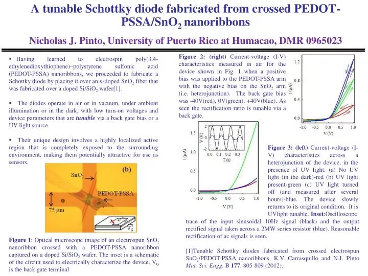
A tunable Schottky diode fabricated from crossed PEDOT-PSSA/SnO2 nanoribbonsNicholas J. Pinto, University of Puerto Rico at Humacao, DMR 0965023 Figure 2: (right) Current-voltage (I-V) characteristics measured in air for the device shown in Fig. 1 when a positive bias was applied to the PEDOT-PSSA arm with the negative bias on the SnO2 arm (i.e. heterojunction). The back gate bias was -40V(red), 0V(green), +40V(blue). As seen the rectification ratio is tunable via a back gate. • Having learned to electrospin poly(3,4-ethylenedioxythiophene)–polystyrene sulfonic acid (PEDOT-PSSA) nanoribbons, we proceeded to fabricate a Schottky diode by placing it over an n-doped SnO2 fiber that was fabricated over a doped Si/SiO2 wafer[1]. • The diodes operate in air or in vacuum, under ambient illumination or in the dark, with low turn-on voltages and device parameters that are tunable via a back gate bias or a UV light source. • Their unique design involves a highly localized active region that is completely exposed to the surrounding environment, making them potentially attractive for use as sensors. Figure 3: (left) Current-voltage (I-V) characteristics across a heterojunction of the device, in the presence of UV light. (a) No UV light (in the dark)-red (b) UV light present-green (c) UV light turned off (and measured after several hours)-blue. The device slowly returns to its original condition. It is UVlight tunable. Inset:Oscilloscope trace of the input sinusoidal 10Hz signal (black) and the output rectified signal taken across a 2MW series resistor (blue). Reasonable rectification of ac signals is seen. [1]Tunable Schottky diodes fabricated from crossed electrospun SnO2/PEDOT-PSSA nanoribbons, K.V. Carrasquillo and N.J. Pinto Mat. Sci. Engg. B 177, 805-809 (2012). Figure 1: Optical microscope image of an electrospun SnO2 nanoribbon crossed with a PEDOT-PSSA nanoribbon captured on a doped Si/SiO2 wafer. The inset is a schematic of the circuit used to electrically characterize the device. VG is the back gate terminal
Undergraduate research presentations at the 2012 APS meeting and the National Conference on Undergraduate Research (NCUR)Nicholas J. Pinto, University of Puerto Rico at Humacao, DMR 0965023 Above: Second year student, William Serrano presents his poster on the fabrication of poly(vinylidene fluoride-trifluoroethylene)/poly(3-hexylthiophene) fibers from tetrahydrofuran at the 2012 NCUR conference in Ogden, UT. His manuscript was accepted for publication in the Conference proceedings and in the journal Ferroelectrics. William is currently in a summer REU program at Penn State University. Another undergraduate, Manuel Bonilla is also currently in a summer REU program at the University of Pennsylvania. Above: Third year student, Luis Pomales presents his work on FET’s made from C-nanotubes covered with poly(3-hexylthiophene) thin films at the annual march meeting of the American Physical Society in Boston, MA.