Download
1 / 23
230 likes | 386 Views
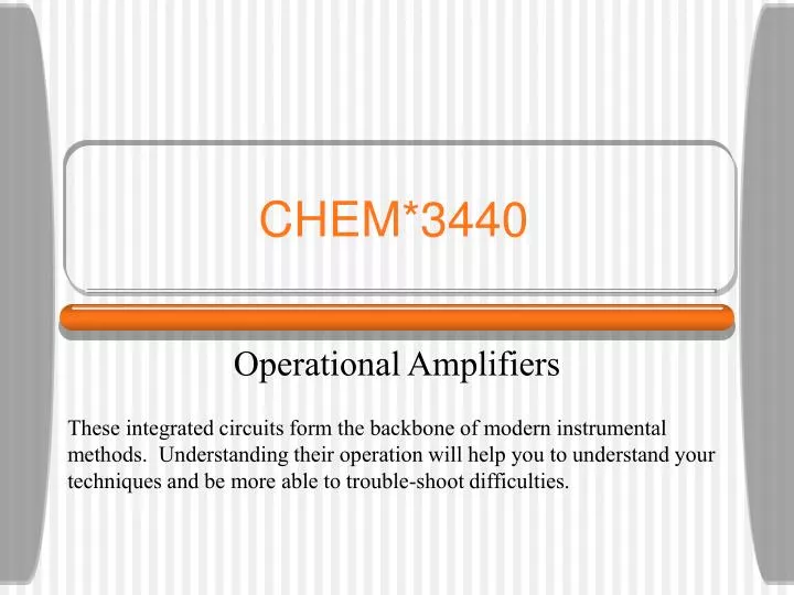
CHEM*3440. Operational Amplifiers. These integrated circuits form the backbone of modern instrumental methods. Understanding their operation will help you to understand your techniques and be more able to trouble-shoot difficulties. Circuit Diagram of 741 Op Amp.

E N D
CHEM*3440 Operational Amplifiers These integrated circuits form the backbone of modern instrumental methods. Understanding their operation will help you to understand your techniques and be more able to trouble-shoot difficulties.
Circuit Diagram of 741 Op Amp Thanks to Tony van Roon in the Electronics Shop for the use of this picture.
Schematic of Op Amp Only three critical connections: • Inverting Input (–) • Non-inverting Input (+) • Output – output +
Important Fundamentals Important basic properties of an Op Amp High input impedance Low output impedance Large gain (104 to 106) Wide unity gain bandwidth Negligible output when inputs are equal Ideal Op Amp ∞ 0 ∞ ∞ 0 Basic operating principles It draws negligible current into its inputs. It will do whatever it can to make the difference between the inputs 0. It is an active device which drives its output from its power supply. Its response is limited by what its power supply can deliver.
The Inputs The notation on the inputs has nothing to do with the polarity of the signal but instead indicates the phase relationship an input signal has with an output signal. – V time + – +
Open Loop Configuration Voutput = b (V+ – V–) Gain b = 106 – V– Voutput + V+ When input difference is 15 µV, the output is 15 V, the power supply maximum. +15 15 µV Open Loop Configuration is not useful. 15 µV –15
Frequency Response of Op Amp Note how the extremely high gain is applicable only at very low frequencies. The gain decreases as the frequency increases. Thanks again to Tony van Roon for the figure.
Closed Loop Configuration Op Amps are employed usefully when the output signal is fed back into one of the inputs through some passive electronic device. diode resistor capacitor wire – V– Voutput + V+
Voltage Follower This configuration uses negative feedback : the output is connected to the inverting input. – b(V+–V– )=Vo but Vo = V– so b(V+–Vo )=Vo bV+=Vo + bVo bV+=(1 + b)Vo But b is huge (106) b (1 + b) V+=Vo V– Voutput + V+ Purpose: A voltage follower buffers a delicate investigation system from a demanding measurement system. Op amp draws negligible input current (not disturbing the investigation system) while being able to deliver significant output current (to meet the demands of the measurement system) in such a way that the output voltage is the same as the input voltage.
Current Amplifier This configuration will convert a small input current into an output voltage that can be easily measured. • iin = i– + ifeed • but i– 0 • iin = ifeed and since V– = V+ = 0 Vo = -if Rf = - iin Rf Rfeedback ifeed iin i– – Iin Vo + If iin = 1 µA and Rf = 100 k, then Vo = 0.1 V = 100 mV
Voltage Amplifier Perhaps the most widely used op amp configuration is that of a voltage amplifier. Rf Vin produces an Iin to flow through Rin. By the same analysis as for the current amplifier, we find that Vin / Rin = – Vo / Rf or Vo = – [Rf/Rin] Vin Rin – Vin Vo + The output voltage is scaled to the input voltage by the ratio of the two resistors. The gain of the circuit is now controlled by the resistor values and not the inherent op amp open loop gain. If Rf is larger than Rin, we have an amplifier; if Rf is less than Rin, we have an attenuator.
Integrator The input current demands a matching feedback current which is delivered by the op amp by changing the output voltage. Cf Rin Reset switch – Vin Vo + The reset switch discharges the capacitor and prepares the circuit for another charging cycle.
Differentiator By switching the capacitor and resistor in the integrator circuit, we obtain a differential response for the output voltage. Rf Vo(t) = – Rf Cin dVin(t)/dt Cin – Vin Vo + The output voltage is large when the rate of change of the input voltage is large. This circuit can be used for detecting “spikes” in a signal that need to be identified or guarded against or eliminated.
Logarithmic Amplifier Many chemical properties have an exponential response (think pH, for example). This circuit can nicely linearize such a response. diodef Vo – log(Vin/Rin) Rin – Vin Vo + By switching the diode and resistor, we can make an antilogarithmic (exponential) amplifier. Circuits are more commonly made using a transistor instead of a diode.
Comparator A useful circuit that answers the question “Is the input voltage greater than or less than a given reference voltage?” Because of the huge open loop gain of the op amp, the output voltage is driven to the power supply limits (±15 V) whenever the input exceeds or remains below the reference voltage. When Vin is on the inverting input, Vo assumes the reverse sign; a non-inverting comparator can be formed by switching the input and reference. Vin – Vo + Vref • This circuit turns a sine wave into a square wave. • Often finds use as a trigger circuit. • Charge a capacitor and feed it back to the reference input – “remembers” peak value.
Summing Amplifier We can run several voltages in parallel to produce a summing effect at the output. R1 Rf V1 R2 – V2 Vo R3 If R1 = R2 = R3 = R then Vo = – [Rf/R] (V1 + V2 + V3) + V3 If R1 = R2 = R3 = Rf then Vo = – (V1 + V2 + V3) If R1 = R2 = R3 = 3Rf then Vo = – [1/3] (V1 + V2 + V3)
log amp log amp antilog amp Multiplying Amplifier By combining a summing circuit with logarithmic and antilogarithmic circuits, we can multiply two voltages together. R R log A A – R AB B + log B log A + log B
Difference Amplifier With this, we can determine the difference between two voltages. Rf R1 = R2 and Rf = R3, then Vo = [Rf/R1] (V2 - V1) R1 – V1 Vo + V2 R2 R1 = R2 = Rf = R3, then Vo = (V2 - V1) R3
log amp log amp antilog amp Dividing Amplifier Combining a difference amplifier with log/antilog circuits allows us to divide to voltages. R R A – B/A + B R R
+ – – – + + Instrumentation Amplifier This is a high precision, very stable difference amplifier which is at the core of most modern instrumental measurements. V1 • Very high CMRR • Fixed, precision, internal gain • Always used as difference amp R6 R2 R4 Vo R1 R3 R5 R7 V2
Example: A Spectrometer A simple spectrometer can be built around an op amp. A photodiode can be used as a transducer; its resistance changes when light impinges on it. Resistance is inversely proportional to the power of the impinging light source. Vo = -(Rref/Rsample) Vsource Vo = k (Psample/Pref) Sample solution Reference solution (blank) Rref Rsample – Vsource Vo +
– + Example: Conductance Cell This is a commonly used detector in devices such as HPLC and ion chromatography and some titrations. In this instrument, note the presence of a standard resistor to regularly calibrate the instrument. The variable resistor can change the gain to cover a larger range of possible cell conductances. Rvariable Rcell rectifier Rstandard meter
Standard temperature 0 ˚C Test temperature ? Example: Thermocouple Thermocouples are used in pairs; the voltage difference is related to the temperature. A difference amplifier is perfect for this job. Vo = [Rf/Rin] (Vt - Vs) T(Vo) Rf Rin Vs copper – Vo constantan copper + Vt Rin Rf