Download
1 / 21
210 likes | 290 Views
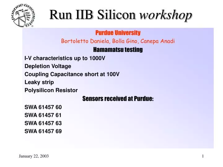
Run IIB Silicon workshop. Purdue University Bortoletto Daniela, Bolla Gino, Canepa Anadi Hamamatsu testing I-V characteristics up to 1000V Depletion Voltage Coupling Capacitance short at 100V Leaky strip Polysilicon Resistor Sensors received at Purdue: SWA 61457 60

E N D
Run IIB Silicon workshop Purdue University Bortoletto Daniela, Bolla Gino, Canepa Anadi Hamamatsu testing I-V characteristics up to 1000V Depletion Voltage Coupling Capacitance short at 100V Leaky strip Polysilicon Resistor Sensors received at Purdue: SWA 61457 60 SWA 61457 61 SWA 61457 63 SWA 61457 69
Run IIB Silicon workshop Purdue Testing results at www.physics.purdue.edu/cdf/Run2B/pres sensor characterization I-V characteristics up to 1000V Depletion Voltage Coupling Capacitance & Oxide Leakage Current Polysilicon Resistor Interstrip Capacitance Radiation Hardness Test sensor SWA61457 60 sensor SWA61457 63 sensor SWA61457 69 have been irradiated at U.C.Davies Irradiation Facility on Sept 27th 2002 fluence = 1.4 1014 1MeV eq-n cm-2 fully characterizated
Run IIB Siliconworkshop Sensor 60 I (120V) =62.6nA hamamatsu I(120V)=77.3nA Sensor 61 I (V=150) =120nA hamamatsu I(150V)=71 nA Sensor 63 I (V=140)=71nA hamamatsu I(140V)=74.3nA Sensor 69 I (140V) =76.8nA hamamatsu I(140V)=81.3nA
Run IIB Siliconworkshop Measurement repeated every 30 min sensor biased at Vbias=200Vexcept when tested Sensor stabilizes in time
Run IIB Siliconworkshop Neutron irradiation fluence 1.4 1014 1MeV n-eq cm^-2 Layer 0 Operating temperature T = -5C (TDR 3-16) Leakage current per strip module Istrip(V > Vd) 95 nA
Run IIB SiliconworkshopNovember 25th, 2002 Annealing procedure 4min @ T=80C sensor 69 Both sensor 60 and sensor 69 I(plateau) 50mA (T = -25C) sensor 60: 1400 min T=20C sensor 69: 800 minT = 20C & annealing Assuming a=410-17 A/cm DI(Vdep) 7mA Measured value DI(Vdep) 5.5mA Estimated Fluence = 1.1 1014 1MeV n-eq Set-up problem
Run IIB Siliconworkshop Sensor at T=-7Cexcept when testing a) Room T -sensor 60 1700min -sensor 63 1200 min -sensor 69 2800 min b) annealing sensor 69 c) measurements taken one month later than previous slide NO breakdown observed Leakage current decreases in time
Run IIB Siliconworkshop Sensor is biased at Vbias=300V No instability is observed
Run IIB Siliconworkshop Sensor 60 Vdep=117 V hamamatsu Vdep=140V Sensor 61 Vdep=141 V hamamatsu Vdep=160V Sensor 63 Vdep=133 V hamamatsu Vdep=160V Hamamatsu values are higher than Purdue measurements Sensor 69 Vdep=132 V hamamatsu Vdep=150V
Run IIB Siliconworkshop ROSE/TN/2000-10 Version 1/14.12/2000 Vd (20C)=Vd(T)*1.0526/[1+A·exp(T/t)] A=0.00936 t = 11.58 Vd(f)=Vd(1kHz)[1-D·log(f/1kHz)] D=0.11+/-0.009 After irradiation Sensor 60 T=-25C,f=1kHz Vdep=137 V T=20C,f=10kHz Vdep=128 V
Run IIB Siliconworkshop After irradiation Sensor 69 T=20C,f=100kHz: Vdep=136 V T=20C,f=10kHz: Vdep =119 V After irradiation & after annealing Sensor 69 to be understood
Run IIB Siliconworkshop After irradiation & after annealing Sensor 69 T=4C,f=1kHz: Vdep=197 V T=20C,f=10kHz: Vdep =176 V measurement performed after 4 months (2800 min at room T)
Run IIB Siliconworkshop Open in the metal ? No evidence after visual inspection At f=100Hz Sensor 60 Coupling Capacitance CC= 134.43+/-0.48pF Sensor 63 Coupling Capacitance CC= 125.32+/-1.99pF Sensor 69 Coupling Capacitance CC= 126.49+/-0.97pF
Run IIB Siliconworkshop Sensor 60 Coupling Capacitance CC= 136.34+/-1.17pF Sensor 69 Coupling Capacitance CC= 134.47+/-5.34pF
Run IIB Siliconworkshop Trend to be understood ? Cint vs bias voltage as expected Sensor 60 Interstrip Capacitance Cint= 3.46+/-1.68pF Sensor 63 Interstrip Capacitance Cint= 3.17+/-0.01pF Sensor 69 Interstrip Capacitance Cint= 3.53+/-0.18pF
Run IIB Siliconworkshop Sensor 63 Interstrip Capacitance Cint= 3.39+/-0.07pF Sensor 69 Interstrip Capacitance Cint= 3.43+/-0.08pF No trend is observed high bias voltage
Run IIB Siliconworkshop Cint vs bias voltage in the region at irregular behavior before irradiation Three different set-up 1. Chuck room T 2. Cold chuck T=12C 3. Environmental chamber T=-25C Oxigen-vacancy generation?
Run IIB Siliconworkshop Measurements one month later than results shown in previous slide Surface charge decays in time
Run IIB Siliconworkshop Before Irradiation Sensor 60 R=1.72 +/- 0.2 MOhm Sensor 63 R=1.84 +/- 0.8 Mohm drop due to positive charge trapped inside SiO2 After Irradiation Sensor 63 R=1.64 +/- 0.04 MOhm Sensor 63 R=1.7 +/- 0.8 Mohm positive charge decay due to thermal annealing tunnel annealing
Run IIB Siliconworkshop Before Irradiation R=1.86 MOhm After Irradiation R=1.71 Mohm measurements affected by high leakage current
Run IIB Siliconworkshop Conclusions We have evaluated the performance of Axial Outer Layer: sensors fulfill the specifications: 1.Leakage Current as Small as expected 2.Bad channel Not found 3.Capacitance Values as Expected 4.Bias Resistor as Expected 5.Full Depletion Voltage after Irradiation as Expected sensor appear easy to charge up bias resistance is affected by positive charge trappped inside SiO2 before irradiation; the effect decreases after irradiation due to positive charge decay (thermal annealing; tunnel annealing) interstrip capacitance is affected by dioxide defects generated during irradiation; these defects decay in time Hamamatsu sensors are radiation hard up to F=1.4*1014 1MeV eq-n cm-2