Download
1 / 9

E N D
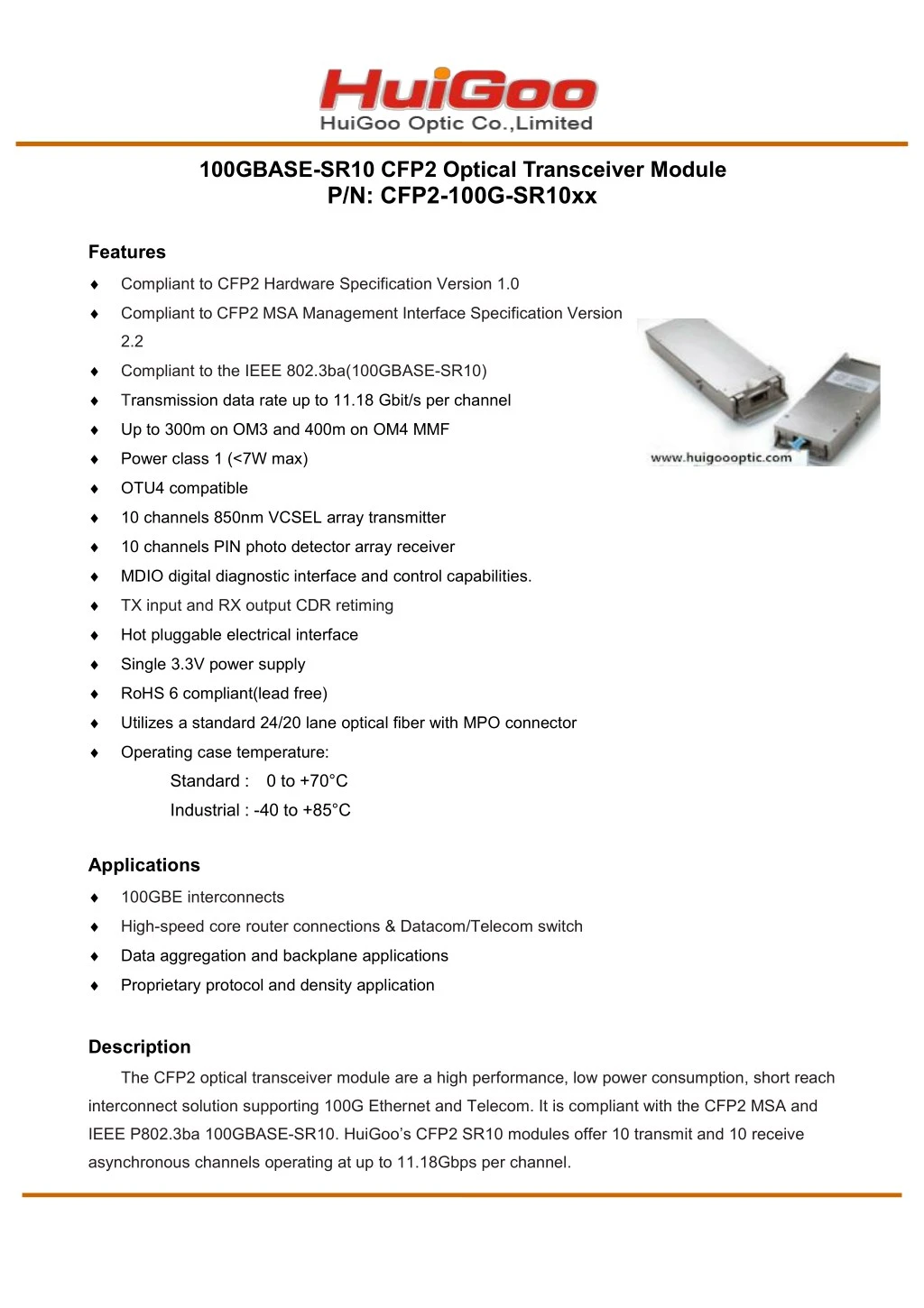
100GBASE-SR10 CFP2 Optical Transceiver Module P/N: CFP2-100G-SR10xx Features Compliant to CFP2 Hardware Specification Version 1.0 Compliant to CFP2 MSA Management Interface Specification Version 2.2 Compliant to the IEEE 802.3ba(100GBASE-SR10) Transmission data rate up to 11.18 Gbit/s per channel Up to 300m on OM3 and 400m on OM4 MMF Power class 1 (<7W max) OTU4 compatible 10 channels 850nm VCSEL array transmitter 10 channels PIN photo detector array receiver MDIO digital diagnostic interface and control capabilities. TX input and RX output CDR retiming Hot pluggable electrical interface Single 3.3V power supply RoHS 6 compliant(lead free) Utilizes a standard 24/20 lane optical fiber with MPO connector Operating case temperature: Standard : 0 to +70°C Industrial : -40 to +85°C Applications 100GBE interconnects High-speed core router connections & Datacom/Telecom switch Data aggregation and backplane applications Proprietary protocol and density application Description The CFP2 optical transceiver module are a high performance, low power consumption, short reach interconnect solution supporting 100G Ethernet and Telecom. It is compliant with the CFP2 MSA and IEEE P802.3ba 100GBASE-SR10. HuiGoo’s CFP2 SR10 modules offer 10 transmit and 10 receive asynchronous channels operating at up to 11.18Gbps per channel. wwwwww
As shown in Figure 1, the transmitter side of the module consists of an array of VCSELs (Vertical Cavity Surface Emitting Lasers) and associated circuitry, which converts 10 parallel electrical data inputs to 10 parallel optical data output signals and also converts 10 parallel optical signals into 10 parallel electrical signals through an array of PIN photodiodes and associated circuitry. Figure1.Module Block Diagram Absolute Maximum Ratings Parameter Symbol Min Max Unit Supply Voltage Vcc -0.5 3.6 V Input Voltage Vin -0.3 Vcc+0.3 V Storage Temperature Tst -40 85 ºC Humidity(non-condensing) *Exceeding any one of these values may destroy the device immediately Rh 5 85 % wwwwww
Recommended Operating Conditions Parameter Symbol Min Typical Max Unit Supply Voltage Vcc 3.13 3.3 3.47 V Operating Case temperature Tca 0 70 ºC Data Rate Per Lane fd - 10.3125 11.18 Gbps Power Dissipation Pm 7 W Low Power Mode Dissipation Plow 2 W Aggregate Bit Rate BRaggr 103.125 111.8 Gbps Electrical Characteristics Parameter Notes Symbol Min Typical Max Unit Differential input impedance Differential Output impedance Differential input voltage amplitude Differential output voltage amplitude Zin 90 100 110 ohm Zout 90 100 110 ohm ΔVin 120 820 mVp-p ΔVout 300 820 mVp-p 3.3V LVCOMS 2.0 VCC+0.3 V Input Logic Level High VIH 1.2V LVCOMS 0.84 1.2 V 3.3V LVCOMS -0.3 0.8 V Input Logic Level Low VIL 1.2V LVCOMS -0.3 0.36 V 3.3V LVCOMS VCC-0.2 VCC V Output Logic Level High VOH 1.2V LVCOMS 1.0 1.5 V 3.3V LVCOMS 0 0.2 V Output Logic Level Low VOL 1.2V LVCOMS -0.3 0.2 V Note: 1. 2. : Differential input voltage amplitude is measured between TxnP and TxnN. Differential output voltage amplitude is measured between RxnP and RxnN. wwwwww
Optical Characteristics Transmitter Optical Specifications (T = 25°C, VCC =3.3V +/- 5%) Parameter Symbol Min Typical Max Unit Average Optical Power(per channel) Pout -7.6 -1 +2.4 dBm Average Optical Power(per channel) - Disabled Poff -30 dBm Optical Return Loss Tolerance 12 dB Extinction Ratio ER 3 dB Center Wavelength λc 840 850 860 nm RMS Spectral Width λ 0.5 0.65 nm Transmit OMA,per Lane TX_OMA/lane -5.6 3 dBm Difference in launch power between any two lanes(OMA) 4 dB Transmitter and dispersion penalty,each lane TDP/lane 3.5 dB Transmitter eye mask Compliant to IEEE802.3ba eye mask specification Note: 1. : Average optical power is measured at the output of the modules optical interface. Receiver Optical Specifications (T = 25°C, VCC =3.3V +/- 5%) Parameter Symbol Min Typical Max Unit Optical Power Sensitivity(per channel) Pin min - -12 -9.9 dBm Optical Power Saturation(per channel) Pin max +1 - - dBm Stressed Receiver Sensitivity PS - - -5.4 dBm Center Wavelength λc 840 850 860 nm RMS Spectral Width λ 0.5 0.65 nm Optical Return Loss Rl 12 dB Damage Threshold 3.4 dBm Optical modulation amplitude,each lane 3 dBm Note: : Optical power sensitivity is measured with BER@10-12at 10.3125Gbps per channel. 1. wwwwww
Pin Descriptions Part A:Bottom Row Pin Function Definition Pin Symbol Type I/O Description 1 GND 2 3 4 TX9n TX9p GND CML CML I I Transmit data input Transmit data input 5 TX8n CML I Transmit data input 6 TX8p CML I Transmit data input 3.3V Module Supply Voltage Return Ground, can be separate or tied together with Signal Ground 7 GND 8 3.3V_GND 9 3.3V 10 3.3V 11 3.3V 12 3.3V 13 3.3V_GND 14 3.3V_GND 15 VND_IO_A I/O Module vendor I/O A. 16 VND_IO_B I/O Module vendor I/O B. Programmable Control 1 set via MDIO, MSA default: TRXIC_RSTn – TX & RX IC reset. “0” = reset, “1” or NC = enabled or not used Programmable Control 2 set via MDIO, MSA default: Hardware Interlock LSB, “00” ≤3W, “01” ≤6W, “10” ≤9W, “11” or NC ≤12W= not used Programmable Control 3 set via MDIO, MSA default: Hardware Interlock MSB, “00” ≤3W, “01” ≤6W, “10” ≤9W, “11” or NC ≤12W= not used Programmable Alarm 1 set via MDIO, MSA default:HIPWR_ON, “1” = Module high power up completed, “0” = Module not high powered up Programmable Alarm 2 set via MDIO,MSA default: MOD_READY,“1” = ready, “0” = not ready Programmable Alarm 3 set via MDIO, MSA default: MOD_FAULT, module fault detected, “1” = fault, “0” = no fault LVCMOS w/PU LVCMOS w/PU LVCMOS w/PU 17 PRG_CNTL1 I I 18 PRG_CNTL2 I 19 PRG_CNTL3 20 PRG_ALRM1 LVCMOS O 21 PRG_ALRM2 LVCMOS O 22 PRG_ALRM3 LVCMOS O 23 GND GND LVCMOS w/PU Transmitter Disable for all channels, “1” or NC = transmitter disabled, “0” = transmitter enabled Receiver loss of optical signal on any channel, “1” = loss of signal, “0” = normal condition Module low power mode. “1” or NC = module in low power (safe) mode, “0” = power-on enabled Module Absent. “1” or NC = Module absent, “0” = module present. Pull-up resistor on Host Module Reset. “0” = reset the module, “1” or NC = module enabled, Pull Down resistor in module Global Alarm. “0” = alarm condition in any MDIO alarm register, “1” = no alarm .Pull-up resistor on Host 24 TX_DIS I 25 RX_LOS LVCMOS O LVCMOS w/PU 26 MOD_LOPWR I 27 MOD_ABS GND O LVCMOS w/PD 28 MOD_RSTn I 29 GLB_ALRMn LVCMOS O 30 GND 31 MDC 1.2V CMOS I Management data clock (electrical specs as per IEEE std802.3-2012) Management Data I/O bi-directional data (electrical specs as IEEE std802.3-2012) 32 MDIO 1.2V CMOS I/O wwwwww
MDIO port address bit 0 33 PRTADR0 1.2V CMOS I MDIO port address bit 1 34 PRTADR1 1.2V CMOS I MDIO port address bit 2 35 PRTADR2 1.2V CMOS I 36 VND_IO_C I/O Module vendor I/O C. 37 VND_IO_D I/O Module vendor I/O D. 38 VND_IO_E I/O Module vendor I/O E. 39 3.3V_GND 40 3.3V_GND 41 3.3V 3.3V Module power Supply 42 3.3V 43 3.3V 44 3.3V 45 3.3V_GND 46 GND 47 RX9n CML O Received data output 48 49 50 RX9p GND RX8n CML O Received data output CML O Received data output 51 RX8p CML O Received data output 52 GND Part B:Top Row Pin Function Definition Pin Symbol Pin Symbol 104 GND 78 REFCLKp 103 TX7n 77 GND 102 TX7p 76 RX7n 101 GND 75 RX7p 100 TX6n 74 GND 99 TX6p 73 RX6n 98 GND 72 RX6p 97 TX5n 71 GND 96 TX5p 70 RX5n 95 GND 69 RX5p 94 TX4n 68 GND 93 TX4p 67 RX4n 92 GND 66 RX4p 91 TX3n 65 GND 90 TX3p 64 RX3n 89 GND 63 RX3p 88 TX2n 62 GND 87 TX2p 61 RX2n 86 GND 60 RX2p wwwwww
85 TX1n 59 GND 84 TX1p 58 RX1n 83 GND 57 RX1p 82 TX0n 56 GND 81 TX0p 55 RX0n 80 GND 54 RX0p 79 REFCLKn 53 GND Figure2. Pad Layout of the CFP2 module CFP2 Optical Interface lanes and Assignment Figure 3 shows the orientation of the multimode fiber facets of the optical connector. Figure3. Outside view of the CFP2 module MPO receptacle Lane Assignment Corresponding Electrical pins Corresponding Electrical pins Fiber Symbol Fiber Symbol 1 Unused 13 Unused 2 RX0 54, ,55 14 TX0 81, ,82 3 RX1 57, ,58 15 TX1 84, ,85 4 RX2 60, ,61 16 TX2 87, ,88 5 RX3 63, ,64 17 TX3 90, ,91 6 RX4 66, ,67 18 TX4 93, ,94 7 RX5 69, ,70 19 TX5 96, ,97 8 RX6 72, ,73 20 TX6 99, ,100 9 RX7 75, ,76 21 TX7 102, ,103 10 RX8 50, ,51 22 TX8 5, ,6 11 RX9 47, ,48 23 TX9 2, ,3 12 Unused 24 Unused wwwwww
Mechanical Dimensions wwwwww
Regulatory Compliance HuiGoo optic transceiver is designed to be Class I Laser safety compliant and is certified per the following standards: Feature Agency Standard Laser Safety FDA CDRH 21 CFR 1040 annd Laser Notice No. 50 Product Safety UL UL and CUL EN60950-2:2007 Environmental protection SGS RoHS Directive 2002/95/EC EN 55022:2006+A1:2007 EN 55024:1998+A1+A2:2003 EMC WALTEK HuiGoo’s 100GBASE-SR10 CFP2 Ordering information Part Number CFP2-100G-SR10 CFP2-100G-SR10I Product Description CFP2,100GBASE-SR10, 300m on OM3 MMFand 400m on OM4 MMF,0 to +70°C CFP2,100GBASE-SR10, 300m on OM3 MMFand 400m on OM4 MMF,-40 to +85°C Important Notice Performance figures, data and any illustrative material provided in this data sheet are typical and must be specifically confirmed in writing by HuiGoo, they become applicable to any particular order or contract. In accordance with the HuiGoo policy of continuous improvement specifications may change without notice. The publication of information in this data sheet does not imply freedom from patent or other protective rights of HuiGoo or others. Further details are available from any HuiGoo’s sales representative. wwwwww