Download
1 / 21
240 likes | 404 Views
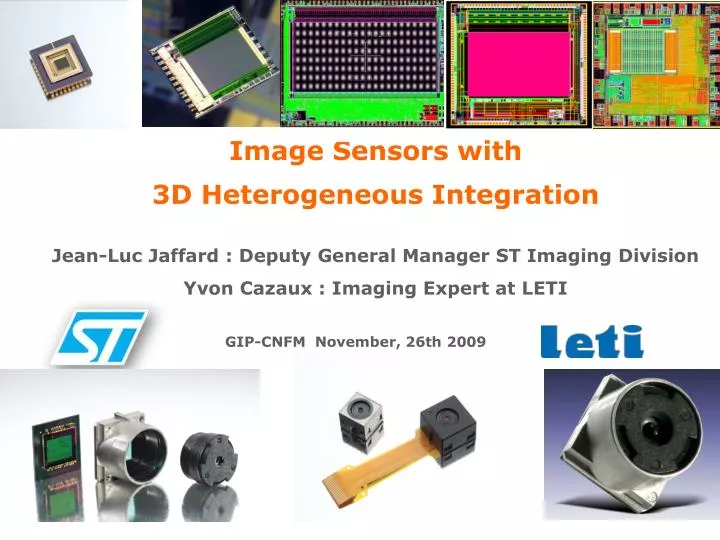
Image Sensors with 3D Heterogeneous Integration. Jean-Luc Jaffard : Deputy General Manager ST Imaging Division Yvon Cazaux : Imaging Expert at LETI. GIP-CNFM November, 26th 2009. Main Applications-Visible Domain. Mobile Phone By far the dominant market Webcam Digital camera

E N D
Image Sensorswith 3D Heterogeneous Integration Jean-Luc Jaffard : Deputy General Manager ST Imaging Division Yvon Cazaux : Imaging Expert at LETI GIP-CNFM November, 26th 2009
Main Applications-Visible Domain • Mobile Phone • By far the dominant market • Webcam • Digital camera • Biomedical (endoscopes) • Automotive : emerging market
Resolution Pixel size Module height Optics 3D INTEGRATION ARENA Physical Size Low Light SNR ratio Crosstalk Speed Process complexity 200mm 300mm 90nm ; 65nm FSI vs BSI ….. Cost Performances Mobile Imaging Driving Factors
VGA Module Size Evolution 8µm pixel Fixed focus Two element lens 1.xµm pixel Wafer level optics 3D Integration Cubic Centimeter
Optical Design Mechanical Design START N Y Y N Y Y N Y=X²+Z+16 Y N N Y STOP Silicon Design Algorithms R&D Challenges : Mastering key technologies
Pixel Size vs Years Pixel size (mm) year 1.75T Pixel 4T Pixels with MOS sharing 2.5T Pixel 3T Pixel 4T Pixel PN Photodiode Photodiode with charge transfer Very Fast Market Evolution • Cost reduction • Always more pixels (5MPix,8MPix, 12MPix…) Smaller and smaller pixel size • Race for miniaturization • Electrical and Optical Integration • Many challenges for CMOS technologies • Lack of sensibility • Temporal & Fix Pattern Noises • Dark Current • Dynamic Range Dedicated Imaging Process
SOURCE IEDM2006_ ST Microelectronics Bayer pattern Mains Challenges for Performances • Sensitivity as high as possible • Large Photodiode (MOS sharing) • mlens to focus photons on the photodiode • Very small dielectric stack, Light Guide, Back side illumination… • Noise Reduction • Dark Current optimization • Fix and Random Readout Noises reduced with Double Correlated Sampling (CDS) • High Signal to Noise Ratio (SNR) • Dynamic Range • Very Small Pixel Capacitance (~1fF) • A Few thousands of electrons at Saturation level • Crosstalk • Optical : Light Diffraction, reflexion on metal lines • Electrical : Carriers Diffusion in the epitaxial layer Colour Crosstalk
Source STMicro. Back Side Illumination • The Way for very Small Pixels to collect all Photons • QE improvement • Less sensitive to the optical aperture (metal lines shading in front side) • Pros • High Sensitivity (~100% Fill Factor) • Suitable to Large Optical Apertures • Cons • Process Complexity • Crosstalk more critical • Cost
CMOS Process Imager options Imager Process CMOS Capable Imager process evolution µm
YUV Raw Bayer Product spec – standards, interfaces Partitioning of a CMOS sensor-based imaging system Frame Store A D C Colour Processor Compression (MPEG4) Data Format Tx Rx System Interface Video Processor System Interface Sensor Module Cable or Flex Connector Possible levels of integration using CMOS technology
TSV based package Through Silicon Interconnect Image Sensor Bump Through Silicon Via Concept • Wire bonding based package Al Pad Wire Bond Image Sensor Package Lead
Through Silicon Via Pros and Cons • Pros • Allow smaller package outline • No pad extension needed • Wire bonding compatible layout • Better density • Cons • More complex technology • Glass • Silicon • Back-end processes • Cost Through via contacts From top to bottom
Swb4 = (Xs+Wb+Lm)² Swb2 = (Xs+Wb+Lm) x (Xs+Lm) VGA Stsv= Xs² 3MP Xs=sqrt (Sensor surface) 5MP Wb Lm Wirebond and TSV modules Physical dimensions comparison WB vs TSV module size Image Sensor Surface (mm²)
Optical Integration at the Wafer Level Conventional module Source: http://www.polight.no Autofocus with piezo actuator • Principle • Lens stacks manufactured at the Wafer level • Dicing of a total Module • Main benefits compared to conventional modules: • Lower Cost • Compact size (die size footprint) • Low building height • Very accurate alignment • Current and Future Developments • Fixed focus • Auto focus • image stabilization devices • Zoom
3D CMOS Integration at the Wafer Level Cu-Cu molecular bonding 3D with TSV (MIT-USA) Photodetection A to D Converter Processor • Principle • CMOS wafers stacking • Electrical connexion between wafers • TSV • Molecular Bonding • Benefits • Compact camera • Processing close to the pixel array • Processor integrated in the BSI handler • New Architecture capability (smart sensors) • Cons • Complex Assy Process • Cost • Yield
TSV image sensor Lenses Image processing Image memory Camera Module Future Integration3D Heterogeneous • Benefits • Physical size • High precision environment • Assembly rules • Clean environment • Simplified test flow • Technical challenges • Manufacturing yield • Mechanical and thermal effects • Optical performances • Dicing • Cost
Conclusions • Addressing Imaging Market means mastering multiple technologies • µelectronics • µoptics • µmechanics • Image processing • Physical size reduction introduces more dependancies between elements and technologies • 3D integration is even more demanding for multiple technology mastering