Download
1 / 3
30 likes | 36 Views
Most group II-VI compounds are direct band gap semiconductors with high optical absorption and emission coefficients .Cadmium Selenide is a leading candidate with high potential towards many applications. The authors present their investigations dealing with preparation and some electrical characterization of the CdSe thin films. The films were deposited onto a well-cleaned glass substrates using thermal evaporation technique. The dependence of electrical resistivity of CdSe thin film in low temperature range has been studied. R.K.Shah | H.O.Parmar | H.S.Patel"On the low temperature resistivity measurement of CdSe thin film" Published in International Journal of Trend in Scientific Research and Development (ijtsrd), ISSN: 2456-6470, Volume-1 | Issue-2 , February 2017, URL: http://www.ijtsrd.com/papers/ijtsrd65.pdf http://www.ijtsrd.com/other-scientific-research-area/physics/65/on--the-low-temperature-resistivity-measurement-of-cdse-thin-film/rkshah<br>

E N D
International Journal of Trend in Scientific Research and Development, Volume 1(2), ISSN: 2456-6470 www.ijtsrd.com On the low temperature resistivity measurement of CdSe thin film R.K.Shah1*,H.O.Parmar1, H.S.Patel2,R.J.Pathak3,V.M.Pathak4 1Arts, Science and R. A. Patel Commerce College, Bhadran, Dist. Anand, Gujarat. 2 Arts,Science and Commerce College, Borsad, Dist. Anand, Gujarat. 3R.R.Mehta College of Science, Palanpur , Dist.Banaskantha, Gujarat. 4Departmentment of Physics, Sardar Patel University, Vallabh Vidyanagar, Gujarat. Abstract: Most group II-VI compounds are direct band gap semiconductors with high optical absorption and emission coefficients .Cadmium Selenide is a leading candidate with high potential towards many applications. The authors present their investigations dealing with preparation and some electrical characterization of the CdSe thin films. The films were deposited onto a well-cleaned glass substrates using thermal evaporation technique. The dependence of electrical resistivity of CdSe thin film in low temperature range has been studied. characterization of any material is very important because it gives an idea about various important parameters related to the material. On the basis of this ,in the present paper ,the authors present their investigations on the preparation of CdSe thin films and the effect of low temperature on the electrical resistivity of the CdSe thin films. EXPERIMENTAL Keywords: Cadmium Selenide, thermal evaporation technique, thin film, electrical resistivity The deposition technique can be chosen depending upon the type of material and its intended use for various applications. The physical vapour deposition technique is the simplest and widely used technique for deposition of semiconducting thin films. The same technique i.e. the thermal evaporation technique has been adopted here for the deposition of CdSe thin films. Stoichiometric CdSe powder having purity around 99.99% was kept in a molybdenum boat. Thin film of CdSe have been deposited at a pressure better than 10-5torr in a vacuum coating unit (Hind High Vac, Bangalore, India).The deposition of the thin films has been carried out on a pre-cleaned glass slides used as the substrates. Prior to deposition, the glass slides were cleaned with acetone which was followed by the washing with distilled water. The thickness has been controlled during the deposition process & measured using quartz crystal thickness monitor. The thickness of the film has been found to be 3kÅ. INTRODUCTION Group II-VI compounds have been studied intensively recently because of their potentials for wide range of applications. These compounds has been studied in crystal as well as thin film form .This is because large uniform areas would prove extremely useful in the preparation of image intensifiers and photo voltaic devices. Amongst these Group II-VI compounds Cadmium Selenide (CdSe) is an important and most promising material .In the much current research ,researchers are interested to understand different properties of Cadmium Selenide from its applications point of view such as thin film transistors[1],thin film solar cells[2-3], photodetectors[4-5],heterojunction solar cells[6] and various optoelectronic devices[7].Several methods have been applied for the preparation of CdSe thin films such as vacuum evaporation technique[8-10], deposition[11], chemical deposition[12-15],SILAR method and electrodeposition method[17-18].Much current research has focused on electrical properties of CdSe thin films. The electrical The variation in electrical resistivity with temperature in a low temperature range has been investigated on CdSe thin films using van der Pauw method. The contacts have been prepared using silver paste. These investigations have been carried out below room temperature using liquid N2 cryostat. The resistivity has been measured within the temperature range from 223 K-300 K. The temperature was controlled and monitored using the cryocontroller throughout the investigations. chemical vapor 28 IJTSRD | Jan-Feb 2017 Available Online@www.ijtsrd.com
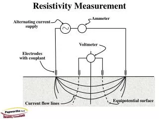
International Journal of Trend in Scientific Research and Development, Volume 1(2), ISSN: 2456-6470 www.ijtsrd.com RESULT AND DISCUSSION CdSe thin films at low temperature ranging from 223 K - 300 K. The experimental set up explained above has been used for CdSe thin films have been obtained in present investigations these investigations. The results obtained for CdSe thin films using the physical vapour deposition technique having thickness apparently show that as the temperature decreases, the around 3000 Å. The thoroughly pre-cleaned micro glass slides resistivity increases, as expected according to the have been used as substrates. The van der Pauw method has semiconducting behaviour of cadmium selenide. been used to study the behaviour of the electrical resistivity of 3.1 2.9 2.7 ln r r 2.5 2.3 2.1 0.0032 0.0036 0.004 0.0044 1/T(K-1) Fig 1. The graph of lnρ vs 1/T 29 IJTSRD | Jan-Feb 2017 Available Online@www.ijtsrd.com
International Journal of Trend in Scientific Research and Development, Volume 1(2), ISSN: 2456-6470 www.ijtsrd.com The graphical representation of the results has been shown in and Sargent E.H., Nature, 2006, 442,180–183. Fig. 1 which is again depicting a non-linear behaviour. This [6] L. Tian; H. Yang; J. Ding; Q. Li;Y. Mu and Y. Zhang, Curr. Appl. Phys., 2014, 14, 881. non-linear behaviour has also been attributed to the hopping [7] V.Saaminathan and K.R.Murali, 2005, J.Cryst.Growth, 2005, 279,229-240. of carriers, the presence of exciton mechanism etc. Moreover from this graph the activation energy of the charge [8] N.C. Parakh and J.C. Garg Indian J. Pure & Appl. Phys., 24 (1986) 154. carriers has been calculated and has found to be around 0.1 [9] F. Raoult, B. Fortin and Y. Colin Thin Solid Films, 182 (1989) 1. eV within the range of temperature under investigations. Besides this the nature of the graph clearly indicates that the CdSe thin films prepared using thermal evaporation technique in [10] A.O. Oduor and R.D. Gould Thin Solid Films, 317 (1998) 409. present investigations exhibits semiconducting behavior. CONCLUSION [11] T.M. Razikov Thin Solid Films, 164 (1988) 301. The present study indicates that the physical vapour deposition [12] F. Trojanek, R. Cingolani, D. Cannoletta, P. Nemee, E. Uhlirova, J. Rohovec and P. Maly technique can be successfully employed for the preparation of CdSe thin films on glass substrates. CdSe thin films having J. Cryst. Growth (Netherlands), 209 (2000) 695. thickness 3kÅ in present investigations possess activation energy [13] S.S. Kale and C.D. Lokhande Mater. Chem. Phys. (Switzerland), 62 (2000) 103. 0.1eV and shows a semiconducting behaviour at low temperature range. [14] O. Savadogo Sol. Energy Mater. Sol. Cells (Netherlands), 52 (1998) 361. REFERENCES [1] Van Claster A; Vervact A.; De Rycke J. and Bates J.D., J.Cryst. Growth, 1998, 86,924. [15] O. Portillo - Moreno, O. Zelaye - Angel, R. Lozada Morales and M. Rubin - Falfan [2] S. M. Pawar; A.V. Moholkar; K.Y. Rajpure and C. H. Bhosale, Opt. Mater. (Netherlands), 18 (2002) 383. Sol. Energy Mater. Sol. Cells,2008, 92, 45-49. [16] Yunus Akathun; M.Ali Yildirim; Aytune Ates and Muhammet Yildirim.Optics [3] P. Mahawela; S. Jeedigunta; S. Vakkalanka; C.S. Ferekides and D. L. Morel Communication, 2008, 284, 2307. Thin Solid Films, 2005, 480-481, 466-470. [17] S. Mishra, R.K. Pandey, P. Sahu, S. Tiwari & B.P. Chandra Sol. Energy Mater. Sol. Cells (Netherlands), 60 (2000) 59. [4] S. Lou; C. Zhou; H. Wang; H. Shen; G. Cheng and Z. Du, Mater. Chem. Phys., 2011, 128, 483-488. [18] V. Subramanian, K.R. Murali & V. Swaminathan Thin solid Films (Switzerland), 359 (2000) 113. [5] Konstantatos G.; Howard I.; Fischer A.; Hoogland S.; Clifford J.; Klem E.; Levina L. 30 IJTSRD | Jan-Feb 2017 Available Online@www.ijtsrd.com