Download
1 / 11
110 likes | 437 Views
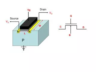
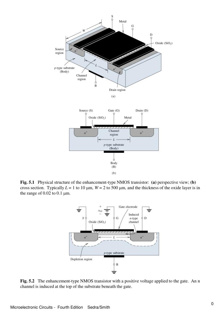
Fig. 5.1 Physical structure of the enhancement-type NMOS transistor: (a) perspective view; (b) cross section. Typically L = 1 to 10 m, W = 2 to 500 m, and the thickness of the oxide layer is in the range of 0.02 to 0.1 m.

E N D
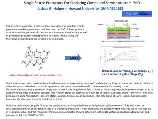
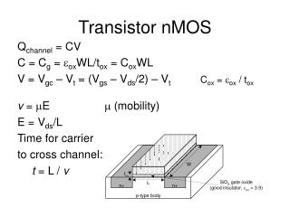
Fig.5.1 Physical structure of the enhancement-type NMOS transistor: (a) perspective view; (b) cross section. Typically L = 1 to 10 m, W = 2 to 500 m, and the thickness of the oxide layer is in the range of 0.02 to 0.1 m. Fig.5.2 The enhancement-type NMOS transistor with a positive voltage applied to the gate. An n channel is induced at the top of the substrate beneath the gate. Microelectronic Circuits - Fourth Edition Sedra/Smith
Fig.5.5 Operation of the enhancement NMOS transistor as vDS is increased. The induced channel acquires a tapered shape and its resistance increases as vDS is increased. Here, vGS is kept constant at a value > Vt. Fig.5.6 The drain current iD versus the drain-to-source voltage vDS for an enhancement-type NMOS transistor operated with vGS > Vt. Microelectronic Circuits - Fourth Edition Sedra/Smith
Fig. 5.55 (a) The CMOS inverter. (b) Simplified circuit schematic for the inverter. Fig. 5.58 The voltage transfer characteristic of the CMOS inverter. Microelectronic Circuits - Fourth Edition Sedra/Smith
Fig. 5.56 Operation of the CMOS inverter when v1 is high: (a) circuit with v1 = VDD (logic-1 level, or VOH); (b) graphical construction to determine the operating point; and (c) equivalent circuit. Fig. 5.57 Operation of the CMOS inverter when v1 is low: (a) circuit with v1 = 0V (logic-0 level, or VOL); (b) graphical construction to determine the operating point; and (c) equivalent circuit. Microelectronic Circuits - Fourth Edition Sedra/Smith
Fig. 5.64 The CMOS transmission gate. Fig. 5.65 Equivalent circuits for visualizing the operation of the transmission gate in the closed (on) position: (a) vA is positive; (b) vA is negative. Microelectronic Circuits - Fourth Edition Sedra/Smith
Fig. 13.3 Definitions of propagation delays and switching times of the logic inverter. Fig. 5.59 Dynamic operation of a capacitively loaded CMOS inverter: (a) circuit; (b) input and output waveforms; (c) trajectory of the operating point as the input goes high and C discharges through the QN; (d) equivalent circuit during the capacitor discharge. Microelectronic Circuits - Fourth Edition Sedra/Smith
Fig. 13.12 A two-input CMOS NOR gate. Fig. 13.13 A two-input CMOS NAND gate. Microelectronic Circuits - Fourth Edition Sedra/Smith
Fig. 13.16 Proper transistor sizing for a four-input NOR gate. Note that n and p denote the (W/L) rations of QN and QP, respectively, of the basic inverter. Fig. 13.17 Proper transistor sizing for a four-input NAND gate. Note that n and p denote the (W/L) rations of QN and QP, respectively, of the basic inverter. Microelectronic Circuits - Fourth Edition Sedra/Smith
Fig. 13.44 A simple implementation of the D flip-flop. The circuit in (a) utilizes the two-phase nonoverlapping clock whose waveforms are shown in (b). Fig. 13.45(a) A master-slave D flip-flop. Note that the switches can be, and usually are, implemented with CMOS transmission gates. (b) Waveforms of the two-phase nonoverlapping clock required. Microelectronic Circuits - Fourth Edition Sedra/Smith
Fig. 14.20 Analysis of the TTL gate with the input high. The circled numbers indicate the order of the analysis steps. Fig. 14.22 Analysis of the TTL gate when the input is low. The circled numbers indicate the order of the analysis steps. Microelectronic Circuits - Fourth Edition Sedra/Smith
Fig. 14.24 The TTL NAND gate. Fig. 14.25 Structure of the multiemitter transistor Q1. Microelectronic Circuits - Fourth Edition Sedra/Smith