Download
1 / 30
310 likes | 479 Views
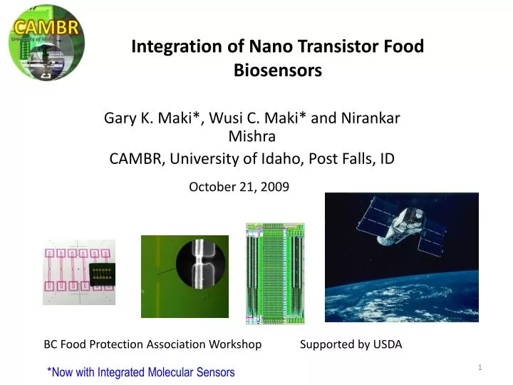
Integration of Nano Transistor Food Biosensors. Gary K. Maki*, Wusi C. Maki* and Nirankar Mishra CAMBR, University of Idaho, Post Falls, ID. October 21, 2009. BC Food Protection Association Workshop Supported by USDA. * Now with Integrated Molecular Sensors.

E N D
Integration of Nano Transistor Food Biosensors Gary K. Maki*, Wusi C. Maki* and Nirankar Mishra CAMBR, University of Idaho, Post Falls, ID October 21, 2009 BC Food Protection Association Workshop Supported by USDA *Now with Integrated Molecular Sensors
Integration of MicroelectronicsCAMBR/NASA Custom Processors • Reed Solomon Coder • Programmable error correction, message length • Lossless Data Compressor (USES) • Low Density Parity Check Encoder • Landsat Data Continuity Mission • High Performance Data Compression • MMS mission • New correlator work underway • GeoStar IIP Delivered November 2008
GeoStar System • The GeoStar system enables astronomers to advance science with a space based imager which will correlate data from 588 separate antennas. • This requires a custom processor board capable of 442,368,000,000,000 correlations per second while using less than 120W for the correlations. • Equivalent to 17,332 Quad Intel Processors consuming 346,600 watts (not counting memory)
Nano Technology Promise • Increased Sensitivity • Electronic device size approximate size of detection molecule • Nano transistors on order of 50 nm capable of manufacture in modern semiconductor foundries • IBM, Intel, TSMC markets 45 nm electronics • With proper integration, possible to mass produce sensitive detection electronics • $20 detectors with integrated microprocessors with USB interfaces
Integration of Electronic Biosensor Nano FET Target Molecule Capture Molecule Self-assembled monolayer Au Au Al Al Silicon Substrate Amplifier Digitizer Computer VSS Off Chip Communications
Pathogen Biomarker Capture & Amplification Detector Sensor Electronic Amplifier Micro processor Communication Link Cell Phone Internet Satellite Computers National Data Base
Technologies/Expertise Molecular Biology/Biochemistry Nano Technology Semiconductor Fabrication Surface Chemistry Electronics Digital Design Analog Design Special purpose computers How to integrate people/technologies
Work Together Multiple disciplinary Speak the same language Substrate Understand basic concepts Cross Knowledge borders Ph.D’s are experts in narrow fields Ph.D’s do not like to show ignorance Chemistry Electronic Engineering Molecular Biology 8
Food Safety Detection Targets • Toxins • SEB SEC (Staph) • Stx1, Stx2 (E. coli) • Bacteria signature DNA • 16S rRNA gene • Bacteria signature RNA • 16S rRNA • E. coli O157:H7 • Specific phage KH1
DNA Bacterium Protein Virus Electronic Molecular Sensor
Bio-molecular Detection on Nano-FET Real Detection Ideal Detection Nano-FET Nano-FET Y Y Y Y Y Y Y Y Nano-FET Nano-FET
Established Bio-Recognition Methods Nano FET Target Molecule Capture Molecule Self-assembled monolayer Au Au Al Al Silicon Substrate Amplifier Digitizer Computer VSS Off Chip Communications
Established Microelectronic Technology Nano FET Target Molecule Capture Molecule Self-assembled monolayer Au Au Al Al Silicon Substrate Amplifier Digitizer Computer VSS Off Chip Communications
Challenges In Signal generation and Interface The interface of Bio-Molecules and Nano-sensing surface Electronic Signal Amplification Digitalization Bio-Molecular Recognition Signal Generation The interface of Nano- and Micro-electronics
Interface Questions Charge must be generated from target recognition How to generate charge? What kind of charge? How much? Charge must be brought to the sensing surface Insulator layer on the nanowire must be as thin as possible How to attach the charge to the surface? How to make ultra-thin insulator layer? Nanowire must be affected by very small E-field Which generates a detectable electronic signal How to integrate nano-/micro-electronics? Temperature and packaging problems Electronic signal is amplified and digitalized Signal level: magnitude only? Phase? Electronic amplify?
Challenges in Charge Generation Not all molecules are alike Charge quantity variable Example Charge sense variation DNA negative charge Poly-lysine positive charge Steroid hormone charge neutral Transistor Impacts Transistor variation with different targets Transistor surface modification
Solution for Charge Generation Keep engineer’s life simple Known amount of charge Known charge sense No transistor surface modification Ease design pain Enable mass production Engineers have to design only one thing and produce billions of identical copies
Universal Signal Molecule Target Recognition Signal Molecule Generation Target Invariant Electronics Same Signal Molecule - known charge
Universal Detection Model Antibody Antigen Y Y Y Signal Molecule PNA Universal Nano-FET Biosensor
Transistor Design Device which detects molecular charge Specifications Wafer Doping level Nanowire Length Contact material Insulator layer Sensing area
Signal Data Nano Transistor nano amp current Noise Problems External noise Light, 60 Hz, electrical ground movement Long wires from nano FET to instrument No alligator clips Internal noise Electrical grounding, cross talk, leakage
Transistor Layout Top View Au Pad Au Pad Doped Silicon Side View Au Pad Au Pad PNA Doped Silicon Insulation Layer Silicon Wafer University of Idaho - CAMBR 22
Areas of Concern High reliability needed Example 0.01% Modern VLSI chip with 100M Xsters 4 contracts per transistor 10,000 Xsters non-functional Contact Side View Au Pad Au Pad PNA Doped Silicon Insulation Layer Silicon Wafer University of Idaho - CAMBR 23
Areas of Concern Nano FET Surface Thickness Small for good E-Field Thick for insulation Thickness Au Pad Au Pad PNA Doped Silicon Insulation Layer Silicon Wafer University of Idaho - CAMBR 24
Au Pad Au Pad Au Pad Au Pad Doped silicon Au Pad Au Pad Doped silicon Au Pad Doped silicon Au Pad Au Pad Doped silicon Au Pad Au Pad Doped silicon Au Pad Au Pad Au Pad Doped silicon Doped silicon Digital Electronics University of Idaho - CAMBR 25
Au Pad Au Pad Au Pad Au Pad Doped silicon Au Pad Au Pad Doped silicon Au Pad Doped silicon Au Pad Au Pad Doped silicon Au Pad Au Pad Doped silicon Au Pad Au Pad Au Pad Doped silicon Doped silicon Digital Electronics Analog Signal to Digital With multiple sensors, quality control routine Data Analysis to map Target Identify Intelligent I/O Interface Internet Communication 26
Au Pad Au Pad Au Pad Au Pad Doped silicon Au Pad Au Pad Doped silicon Au Pad Doped silicon Au Pad Au Pad Doped silicon Au Pad Au Pad Doped silicon Au Pad Au Pad Au Pad Doped silicon Doped silicon • Digital Electronic Problems • Processing Order • Create Digital Circuits (20 layers) • Place Gold pads • Place doped silicon on gold pads • High Temperature Process • Nano packaging solution ? 27
Integration of Nano- and Microelectronics Microelectronics
Hybrid Packaging Approach • Short wire interface • Common ground • Noise reduction elements • Single package Hybrid Package Micro-electronics Nano-device
Conclusion Systems Level Problem Various Technology experts needed Integrated team is needed Resource costs are High nano foundry (already exists) Digital/Analog Design Tools Commercial costs > $1M/year Engineering experts needed Commercial fabrication > $200K/run Biomolecular laboratory