Download
1 / 7
70 likes | 220 Views
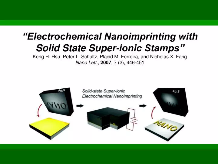
“Electrochemical Nanoimprinting with Solid State Super-ionic Stamps” Keng H. Hsu, Peter L. Schultz, Placid M. Ferreira, and Nicholas X. Fang Nano Lett. , 2007 , 7 (2), 446-451. Electrochemical Micromachining. Comparison of parallel top-down methods used to create metallic nanostructures.

E N D
“Electrochemical Nanoimprinting with Solid State Super-ionic Stamps” Keng H. Hsu, Peter L. Schultz, Placid M. Ferreira, and Nicholas X. Fang Nano Lett., 2007, 7 (2), 446-451
Electrochemical Micromachining Comparison of parallel top-down methods used to create metallic nanostructures • S. Zankovych, T. Hoffman, J. Seekamp, J.U. Brunch, C.M. Torres Nanotechnology 2001, 12, 91-95 • A.L Trimmer, J.L. Hudson, M. Kock, R. Schuster Applied Physics Letters 2003, 82, 3327-3329
Metallic electrode back of stamp (cathode) Stamp: Ag2S solid electrolyte (super-ionic conductor) Patterned material (anode, Ag) Mobile Ag+ ions move through defect lattice and channels to recombine w/ e- at cathode Potential drop at interface causes oxidation of Ag and results in mobile Ag+ ions Stamp released when current approaches zero Solid state super-ionic stamping process Potential between anode and cathode held constant Stamping pressure held constant
Solid state super-ionic stamping: first generation results (B) Stamped 300nm Ag substrate at Vbias=0.8V • FIB etched Ag2S stamp Concentric Circles Pitch: 500 390 240 nm Rectangles 60 nm to 1.3 µm (D) Close up of imprinted letters showing spurs on the surface (C) Perspective view Letters Line width: 200 nm Height: 300nm Keng H. Hsu, Peter L. Schultz, Placid M. Ferreira, and Nicholas X. Fang Nano Lett., 2007, 7 (2), 446-451
Solid state super-ionic stamping: first generation results Stamped 300nm Ag substrate at Vbias=0.3V Line witdths(left to right) 1600 to 60 nm Pitch Top right set: 30 nm Top left set: 50 nm Middle set: 200 nm Bottom set: 350 nm Height 100 nm (60 nm lines only 30 nm) Keng H. Hsu, Peter L. Schultz, Placid M. Ferreira, and Nicholas X. Fang Nano Lett., 2007, 7 (2), 446-451
Increasing dissolution rate with increase in V (dissolution by breaking space charge layer at interface Anodic dissolution switches from charge transfer control to diffusion control) Anodic sweep analysis for Ag dissolution Fall off associated with depletion of Ag substrate Anodic Sweep at 20 mVs-1 Evolution of total current over etch time for stamping process
Conclusions • Potential Drawbacks • Stamp lifetime has not been fully investigated yet • Patterning layers difficult (alignment and anodic contact) • Limited range of materials investigated (Ag, Cu) • Demonstrated Possibilities • Inexpensive • High aspect ratios possible • High resolution (50 nm) • Patterning of acute angles possible (15º) • Conducted in ambient environment • Doesn’t require liquids • Single step patterning Variation in etch time for subsequent runs using same stamp (80 nm substrates)