Download
1 / 23
240 likes | 581 Views
Microanalysis and Metallography. Mentor: Bob Goddard Teachers: Helen Follis and Ann-Marie Bissoo. Outline. Research Experiences Microanalysis - ESEM Metallography - Samples Professional and Personal Impact. Definitions.

E N D
Microanalysis and Metallography Mentor: Bob Goddard Teachers: Helen Follis and Ann-Marie Bissoo
Outline • Research Experiences • Microanalysis - ESEM • Metallography - Samples • Professional and Personal Impact
Definitions • Microanalysis: It is the art of using an electron microscope (ESEM) to view, observe, and interpret micro-structural details seen in objects. • Metallography: Creating samples of materials by using a detailed process of sectioning, sanding, grinding, polishing, finishing, analyzing, and interpreting data.
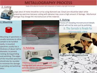
Procedure in making a Sample • Cut wire – approx. 5 mm in length • Hot mount • Sand and Grind - wash • Observe with light microscope – wash • Polish with 9 micron and 3 micron diamond grit – wash • Observe with light microscope - wash • Place in Finisher for final polish with .05 micron diamond grit • Sample may be “finished” between 1 hour to 8 hours - wash • Observe with light microscope and/or electron microscope • Take pictures with varying magnification • Etch with nitric acid for 30 to 45 seconds - wash • Take pictures with light microscope and/or electron microscope • Interpret and extrapolate data. Photograph and/or print procedure • Reassembling individual layers of wire using Adobe Photoshop pictures (Helen) • “Etch-a-Sketch” using layering in Adobe Photoshop (Ann-Marie)
Helen’s Mounted Wire for Sampling Sample mounted in resin Clip to hold wire Wire cross-section taken every 5 mm
Helen’s Research Statement • To determine the microscopic composition of this superconducting wire
Hypothesis • The microscopic distribution of elements and the occurrence of voids determines the strength and electrical properties of the sample.
Wire cross section photographs taken with the light microscope 0.6 mm
ESEM Microanalysis-Overview of grain Copper Matrix Superconducting Niobium Tin Filaments Voided area caused by Tin being diffused out of this area
More detailed view of grain Bronze depleted zone Individual Wires ~2 um Nb/Sn Reacting Zone Copper Matrix
Chemical Results Not Heat Treated Heat Treated 1 2 1 2 3 4 4 3 1: Niobium 2: Copper 3: Tin 4: Line Analysis
Conclusion • The wires were reacted properly because the tin can be seen diffused into the niobium. • The strength and the electrical properties should be suitable for use in high-field magnets. • Separate independent testing of the critical current measurements under stress indicate the wires will perform at the temperature and the strength required.
Ann-Marie’s Research Statement • To determine if a shipment of copper wire is already heat treated and if the individual grains are uniform in size. • This is necessary to determine the suitability of this wire for use in the pulse magnet.
Hypothesis • I believe that the wire is heat treated and that the individual grains are uniform in size.
Ann-Marie’s Mounted Wire for Sampling Resin for Hot Mount Cable of Wire One Piece of Wire Mount = 2.5 cm
Light MicroscopeOne Whole Wire Whole Wire Possible water stain 1.2 mm
Light microscope – etched, partial picture of a wire Light microscope Water Stain Hole caused by etching with Nitric Acid Individual Grain
ESEM Microanalysis One whole wire under the ESEM Not much details
“Etch–a-sketch” Large- sized grain Middle- sized grain Small- sized grains
Result The result showed the following: That the wire grains were not of a uniform size. Avg. Diameter: 15.10 microns
Conclusion • Due to the moderate variation in grain size and the location of the grains, we can conclude that this wire was not heat treated. Therefore, the wire is acceptable for use in the Pulse Magnet. • My hypothesis was wrong.
Professional and Personal Impact • We both agree that this experience has enriched our lives. • Detailed working knowledge of the scientific method • Increased our appreciation for work being conducted in the scientific community • Given us increased understanding and compassion for our students when they say, “I just don’t get it!” • As Louis Armstrong sang, “What A Wonderful World!”
We would like to thank the following… • Robert Goddard • Pat Dixon • Gina LaFrazza • Carlos Villa • Other staff at the NHMFL • National Science Foundation • 2005 RET/REU participants