Download
1 / 75
1.03k likes | 1.78k Views
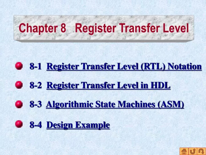
Chapter 8 Register Transfer Level. 8-1 Register Transfer Level (RTL) Notation. 8-2 Register Transfer Level in HDL. 8-3 Algorithmic State Machines (ASM). 8-4 Design Example. Chapter 8 Register Transfer Level. 8-5 HDL Description of Design Example. 8-6 Binary Multiplier.

E N D
Chapter 8 Register Transfer Level 8-1 Register Transfer Level (RTL) Notation 8-2 Register Transfer Level in HDL 8-3 Algorithmic State Machines (ASM) 8-4 Design Example
Chapter 8 Register Transfer Level 8-5 HDL Description of Design Example 8-6 Binary Multiplier 8-7 Control Logic 8-8 HDL Description of Binary Multiplier 8-9 Design with Multiplexers
8-1 Register Transfer Level (RTL) Notation A digital system is a sequential logic system constructed with flip-flops and gates. Because the number of states would be prohibitively large, digital systems are designed using a modular approach instead of state table. Digital modules are best defined by a set of registers and the operations that are performed on the binary information stored in them.
8-1 Register Transfer Level (RTL) Notation A digital system is represented at the register transfer level (RTL) when it is specified by the following three components: • The set of register in the system • The operations that are performed on the data stored in the register. • The control that supervises the sequence of operations in the system.
8-1 Register Transfer Level (RTL) Notation The type of operations most often encountered in digital systems can be classified into four categories: • Transfer operations • Arithmetic operations • Logic operations • Shift operations
8-2 Register Transfer Level in HDL In Verilog HDL, RTL descriptions use a combination of behavioral and dataflow constructs. Register transfers are specified by means of procedural assignment statement. Combinational circuit functions are specified by means of continuous assignment or procedural assignment statement.
8-2 Register Transfer Level in HDL Examples: assign S = A + B; Continuous assignment always @ (A OR B) S = A + B; Procedural assignment ( without a clock ) always @ ( posedge clock) begin RA = RA + RB; RD = RA; end Blocking procedural assignment
8-2 Register Transfer Level in HDL Examples: always @ ( negedge clock) begin RA <= RA + RB; RD <= RA; end Non-blocking procedural assignment
8-2 Register Transfer Level in HDL HDL Operations
8-2 Register Transfer Level in HDL HDL Operations
8-2 Register Transfer Level in HDL HDL Operations
8-2 Register Transfer Level in HDL Loop statements Four types of loops : Repeat, forever, while and for The repeat loop executes the associated statements a specified number of times. initial begin clock = 1'b0; repeat (16); #5 clock = ~ clock; end
8-2 Register Transfer Level in HDL Loop statements The forever loop causes a continuous repetitive execution of the procedural statement. initial begin clock = 1'b0; forever # clock = ~ clock; end
8-2 Register Transfer Level in HDL Loop statements Interger count; initial begin count = 0; while ( count < 64) count = count + 1; end The while loop executes a statement or block of statement repeatedly while an expression is true.
8-2 Register Transfer Level in HDL Loop statements //description of 2x4 decoder //using for-loop statement module decoder (IN, Y); input [1:0] IN; //Two binary inputs output [3:0] Y; //Four binary outputs reg [3:0] Y; integer I; //control variable for loop always @ (IN) for (I = 0; I <= 3; I = I + 1) if (IN == I) Y[I] = 1; else Y[I] = 0; endmodule Output Y is evaluated in a procedural statement, it must be declared as reg type.
8-2 Register Transfer Level in HDL Logic Synthesis Logic synthesis is the automatic process of transforming a high level language description such as HDL into an optimized netlist of gates that perform the operations specified by the source code.
8-2 Register Transfer Level in HDL Logic Synthesis The test bench provides the stimulus signals to the simulator.
8-2 Register Transfer Level in HDL Logic Synthesis If the result of the simulation is not satisfactory, the HDL description is checked again.
8-2 Register Transfer Level in HDL Logic Synthesis If the result of the simulation shows a valid design, the RTL description is applied to the logic synthesizer.
8-2 Register Transfer Level in HDL Logic Synthesis Gate-level circuit simulation
8-2 Register Transfer Level in HDL Logic Synthesis If any corrections are needed, the process will be repeated.
8-3 Algorithmic State Machine (ASM) The logic design of a digital system can be divided into two distinct parts: • Design of the digital circuits that perform the data processing operations. 2. Design of the control circuits that determines the sequence in which the various actions are performed.
8-3 Algorithmic State Machine (ASM) The relationship between two parts is shown as follows, Commands Control logic Data path External input Input data Output data
8-3 Algorithmic State Machine (ASM) A flowchart is a convenient way to specify the sequence of procedural steps and decision paths for an algorithm. A special flowchart called an algorithmic state machine (ASM) chart describes the sequence of events as well as the timing relationship between the states of a sequential controller and the events that occur while going from one state to the next.
8-3 Algorithmic State Machine (ASM) ASM Chart The ASM Chart is composed of three basic elements: the state box, the decision box, and the conditional box. State Box
8-3 Algorithmic State Machine (ASM) Decision Box Conditional Box
8-3 Algorithmic State Machine (ASM) ASM Block The ASM block is a structure consisting of one state box and all the decision and conditional boxes connected to its exit path. The ASM chart is very similar to a state diagram. It is convenient to convert the chart into a state diagram and use sequential circuit procedures to design the control logic.
8-3 Algorithmic State Machine (ASM) State diagram equivalent to the ASM chart ASM Block ASM Block
8-3 Algorithmic State Machine (ASM) Timing Consideration The major difference between a conventional flow chart and an ASM chart is in interpreting the time relationship among the various operations.
8-3 Algorithmic State Machine (ASM) Timing Consideration An ASM chart considers the entire block as one unit. All the operations that are specified within the block must occur in synchronism during the edge transition of the same clock pulse.
8-4 Design Example Design a digital system with two flip-flops, E and F, and one 4-bit binary counter A. the individual flip-flops in A are denoted by A4 ,A3 ,A2 ,A1 , with A4 holding the most significant bit of the count. A start signal S initiates the system operation by clearing the counter A and flip-flop F. the counter is incremented by one starting from the next clock pulse and continues to increment until the operations stop. Counter bit A4 and A3 determine the sequence of operations:
8-4 Design Example Counter bit A4 and A3 determine the sequence of operations: If A3 = 0, E is cleared to 0 and the count continues. If A3 = 1, E is set to 1; then if A4 = 0, the count continues, but if A4 = 1, F is set to 1 on the next clock pulse and the system stops counting. Then if S = 0, the system remains in the initial state, but if S = 1, the operation cycle repeats.
8-4 Design Example ASM Chart
8-4 Design Example Timing Sequence
8-4 Design Example Timing Sequence
8-4 Design Example Datapath Design
8-4 Design Example Register Transfer Representation
8-4 Design Example State Table
8-4 Design Example Control Logic the following equation can be derived from the the state table. DG1 = T1 A3 A4 DG0 = T0 S + T1 T0 = G'0 T1 = G'1 G0 T2 = G1
8-5 HDL Description of Design Example It is the most abstract level. Some of the constructs at this level might not be synthesizable. structural description Three levels of design: RTL description It is the lowest and most detailed level. algorithmic-based behavioral description
RTL Description //RTL description of design example (Fig.8-9) module Example_RTL (S,CLK,Clr,E,F,A); //Specify inputs and outputs //See block diagram Fig. 8-10 input S,CLK,Clr; output E,F; output [4:1] A; //Specify system registers reg [4:1] A; //A register reg E, F; //E and F flip-flops reg [1:0] pstate, nstate; //control register //Encode the states parameter T0 = 2'b00, T1 = 2'b01, T2 = 2'b11; //State transition for control logic //See state diagram Fig. 8-11(a) always @(posedge CLK or negedge Clr) if (~Clr) pstate = T0; //Initial state else pstate <= nstate; //Clocked operations always @ (S or A or pstate) case (pstate) T0: if(S) nstate = T1; T1: if(A[3] & A[4]) nstate = T2; T2: nstate = T0; default: nstate = T0; endcase //Register transfer operatons //See list of operations Fig.8-11(b) always @(posedge CLK) case (pstate) T0: if(S) begin A <= 4'b0000; F <= 1'b0; end T1: begin A <= A + 1'b1; if (A[3]) E <= 1'b1; else E <= 1'b0; end T2: F <= 1'b1; endcase endmodule
Testing the Design Description //Test bench for design example module test_design_example; reg S, CLK, Clr; wire [4:1] A; wire E, F; //Instantiate design example Example_RTL dsexp (S,CLK,Clr,E,F,A); initial begin Clr = 0; S = 0; CLK = 0; #5 Clr = 1; S = 1; repeat (32) begin #5 CLK = ~ CLK; end end initial $monitor("A = %b E = %b F = %b time = %0d", A,E,F,$time); endmodule The Clr signal is set to 0 to initialize the control. The $monitor statement displays the values of A,E,F every 10ns
Structural Description //Structural description of design example //See block diagram Fig. 8-10 module Example_Structure (S,CLK,Clr,E,F,A); input S,CLK,Clr; output E,F; output [4:1] A; //Instantiate control circuit control ctl (S,A[3],A[4],CLK,Clr,T2,T1,Clear); //Instantiate E and F flip-flips E_F EF (T1,T2,Clear,CLK,A[3],E,F); //Instantiate counter counter ctr (T1,Clear,CLK,A); endmodule //Control circuit (Fig. 8-12) module control (Start,A3,A4,CLK,Clr,T2,T1,Clear); input Start,A3,A4,CLK,Clr; output T2,T1,Clear; wire G1,G0,DG1,DG0; //Combinational circuit assign DG1 = A3 & A4 & T1, DG0 = (Start & ~G0) | T1, T2 = G1, T1 = G0 & ~G1, Clear = Start & ~G0; //Instantiate D flip-flop DFF G1F (G1,DG1,CLK,Clr), G0F (G0,DG0,CLK,Clr); endmodule Instantiate three components
Structural Description //Structural description of design example //See block diagram Fig. 8-10 module Example_Structure (S,CLK,Clr,E,F,A); input S,CLK,Clr; output E,F; output [4:1] A; //Instantiate control circuit control ctl (S,A[3],A[4],CLK,Clr,T2,T1,Clear); //Instantiate E and F flip-flips E_F EF (T1,T2,Clear,CLK,A[3],E,F); //Instantiate counter counter ctr (T1,Clear,CLK,A); endmodule //Control circuit (Fig. 8-12) module control (Start,A3,A4,CLK,Clr,T2,T1,Clear); input Start,A3,A4,CLK,Clr; output T2,T1,Clear; wire G1,G0,DG1,DG0; //Combinational circuit assign DG1 = A3 & A4 & T1, DG0 = (Start & ~G0) | T1, T2 = G1, T1 = G0 & ~G1, Clear = Start & ~G0; //Instantiate D flip-flop DFF G1F (G1,DG1,CLK,Clr), G0F (G0,DG0,CLK,Clr); endmodule Describe the control and it D flip-flop
Structural Description //E and F flipf-lops module E_F (T1,T2,Clear,CLK,A3,E,F); input T1,T2,Clear,CLK,A3; output E,F; wire E,F,JE,KE,JF,KF; //Combinational circuit assign JE = T1 & A3, KE = T1 & ~A3, JF = T2, KF = Clear; //Instantiate JK flipflop JKFF EF (E,JE,KE,CLK), FF (F,JF,KF,CLK); endmodule //JK flip-flop module JKFF (Q,J,K,CLK); input J,K,CLK; output Q; reg Q; always @ (posedge CLK) case ({J,K}) 2'b00: Q = Q; 2'b01: Q = 1'b0; 2'b10: Q = 1'b1; 2'b11: Q = ~Q; endcase endmodule //counter with synchronous clear module counter (Count,Clear,CLK,A); input Count,Clear,CLK; output [4:1] A; reg [4:1] A; always @ (posedge CLK) if (Clear) A<= 4'b0000; else if (Count) A <= A + 1'b1; else A <= A; endmodule Describe the E and F and their JK flip-flop
Structural Description //E and F flipf-lops module E_F (T1,T2,Clear,CLK,A3,E,F); input T1,T2,Clear,CLK,A3; output E,F; wire E,F,JE,KE,JF,KF; //Combinational circuit assign JE = T1 & A3, KE = T1 & ~A3, JF = T2, KF = Clear; //Instantiate JK flipflop JKFF EF (E,JE,KE,CLK), FF (F,JF,KF,CLK); endmodule //JK flip-flop module JKFF (Q,J,K,CLK); input J,K,CLK; output Q; reg Q; always @ (posedge CLK) case ({J,K}) 2'b00: Q = Q; 2'b01: Q = 1'b0; 2'b10: Q = 1'b1; 2'b11: Q = ~Q; endcase endmodule //counter with synchronous clear module counter (Count,Clear,CLK,A); input Count,Clear,CLK; output [4:1] A; reg [4:1] A; always @ (posedge CLK) if (Clear) A<= 4'b0000; else if (Count) A <= A + 1'b1; else A <= A; endmodule Describe the counter
8-6 Binary Multiplier When multiplication procedure is implemented with digital hardware, it provides circuits for the summation of only two binary numbers and successively accumulate the partial products in a register. The partial product being formed is shifted to the right. When the corresponding bit of the multiplier is 0, there is no need to add all 0's the partial product.
Multiplicand n Sum Multiplier Product 8-6 Binary Multiplier Register Configuration The P counter is initially set to hold the number of bits in the multiplier and is decremented after formation of each partial product.
Multiplicand n Sum Multiplier Product 8-6 Binary Multiplier Register Configuration The multiplicand is stored in register B.
Multiplicand n Sum Multiplier Product 8-6 Binary Multiplier Register Configuration A parallel adder adds the contents of register B to register A.