Download
1 / 9
90 likes | 217 Views
WP6 interconnect technology part. Slides prepared by Sami Vaehaenen Presented by M. Campbell. WP6 – 3D packaging part. Manpower Sami Vaehaenen CERN Fellow 100% Timo Tick ACEOLE PhD Student 100% Michael Campbell CERN Staff 20%. Recent Actions / Ongoing Work. Low-cost bumping

E N D
WP6 interconnect technology part Slides prepared by Sami Vaehaenen Presented by M. Campbell
WP6 – 3D packaging part • Manpower • Sami Vaehaenen CERN Fellow 100% • Timo Tick ACEOLE PhD Student 100% • Michael Campbell CERN Staff 20%
Recent Actions / Ongoing Work • Low-cost bumping • Single chip Ni/Au UBM depositions were tested for Medipix2 chips at PacTech. • Looking forward to test PacTech’s solder ball placement systems for rapid solder deposition. • There have been negotiations with a Swedish company called “Smoltek” about collaborating with development of state-of-the-art anisotropically conductive films (ACF) for radiation pixel detectors. • Visit at S.E.T. in St Jeoire, the place where the state-of-the-art flip chip bonders are made. • 3D test vehicle • 3d test vehicle has been designed at CERN and it can be used in the development and evaluation of all the three key technologies: through silicon vias (TSV), low cost bump bonding and large-area BGA solder ball interconnections on different substrates. • Test vehicle mask design finished. Waiting for TSV or low-cost bumping technique characterizations (daisy chain, Kelvin via and/or bump measurements. • Through silicon via (TSV) project with VTT (funded by Medipix2 Collaboration) • TSV process development project with VTT has been started and masks are under purchasing process. • Sami and Timo visited VTT to finalize the process flow for dummy wafers. • Substrate technologies • Timo is searching suitable substrate candidates for 3d integrated structures (TSV’s). LTCC and CCL are the most interesting candidates at the moment.
Low-cost Bumping Work at PacTech • PacTech has done some single chip Ni/Au UBM depositions for a handful of Medipix2 chips. • Prototyping process was quickly set up for the chips. There were some issues with plating quality mainly because single chips are more difficult to plate than whole wafers. • It was shown that electroless Ni/Au can be grown uniformly even in very fine-pitch bump layout. • Encouraging results (pictures) were obtained for the use of electroless technology for MPX2. • Test batch of wafers is under preparation for characterization of yields with electroless Ni/Au UBM’s. Electroless plated UBM’s could be used with solder or ACF’s. • Ni/Pd/Au metallization would be most reliable electroless solution Ni is strongly passivated and it will remain solderable even if exposed for elevated temperatures for a long time. • Gang ball placement (GBP) technology is advancing and 40 µm sized solder balls have been tried in process prototyping (animation). • 40 µm sized solder spheres would be suitable for many of CERN’s present day detectors if they could be transferred with high yields (> 99%). PacTech aims at 100% bumping yield with GBP technology because of the visual inspection routine before bonding the solder spheres. Reflow Bonding Flux deposition Cleaning
Smoltek ACF Technology • Smoltek has a very interesting solid carbon nanotube growth process, which can be used in fabrification of sub-micron resolution ACF’s. • Estimated fibre diameters are ≈ 30 nm. Fibres are grown in clusters and the pitch of patterned clusters ≥ 100 nm. • Fibres can be metallized with nickel. • We are looking forward to collaborate with Smoltek. Smoltek would provides the ACF on wafers and CERN would provide the data about the flip chip yields. • ACF fabrication process consist of: • Spinning of liquid catalyte. • Patterning by lithography. • CVD growth of carbon nanotubes at 400 ̊C (≈ 50 nm/min) on patterned areas. • Spinning of polymer on fibres. • Removal of the top surface of the polymer to expose the carbon fibre ends. • Nanofibres can be grown on many materials (Ni, Cu, Al, glass, etc…) • Restriction: only 4” wafers or wafer pieces can be deposited in the chamber at the moment.
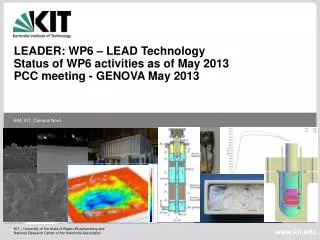
3D Test Vehicle • 3D test vehicle has been designed for characterization of bump bonding, through silicon via and BGA assembly processes. • Aim is to provide feedback for collaborating companies and to acquire reliability data at CERN. • Measurements can be done for daisy chains on three layers, Kelvin bumps at sensor– ROC interface and Kelvin TSV’s on readout chips. Possibility for very demanding through package testing from 4 outputs on carrier. • The layout enables advanced packaging technologies, such as chip-to-wafer and wafer-to-wafer bonding, for future interconnection development. • Benefits • Easily measureable test platform. • Flip chip bonding yield and low-cost bumping technology evaluation. • Via yield and reliability testing. • BGA interface optimization and evaluation. • Development of assembly procedures. • Parallel development of vias, low-cost bumping, re-routing layers and BGA interface. • Create reference comparison between foundries. Probing pads can be diced off for 2D tiling of structures.
Potential Substrate Technologies for 3D • Glass epoxy laminates (FR4): Traditional circuit board • Cheap and very mature technology • High density wiring (HDI built-up technology) • Low Temperature Cofired Ceramics (LTCC): Multilayer ceramic circuit board • Mature technology • High density wiring • Carbon Composite Laminates (CCL): FR4 board with carbon composite sheets • Compatible with traditional process -> cheap • Compatible with HDI built-up technology
TSV Development Project with VTT • Medipix2 collaboration has started a TSV development project with VTT. The aim is at developing a Cu TSV process, which could be later used in production of detector assemblies. • In the beginning, process is developed with blank wafers. After establishing a TSV process, we will proceed with the real process wafers. • The complete 3D integration process is complex and many process entities have to be at good level to build an operational device in the end. • Via filling plays the most demanding role in 3D integration process • 3D test vehicle for electrical measurements will be created by CERN, which is used for characterization of processes. • Process flow for dummy wafers was finalized at VTT in the end of May.
Actions to Come • Batch of test vehicle wafers has to be prepared for the low cost bumping work. • UBM depositions will be continued at PacTech. • Prototyping with gang ball placement technology at PacTech. • Test state-of-the-art anisotropically conductive adhesives for flip chip. • Smart Equipment Technology (S.E.T.) should provide some simulation results for advanced flip chip bonding systems. • 32 pin probe card has to be designed and ordered for the 3D test vehicle. • Looking forward to first TSV wafers processed by VTT. • Sami and Timo are in Electronics Components Technology Conference in San Diego, U.S.