Download
1 / 25
550 likes | 1.36k Views
Etching of High Aspect Ratio Trenches Abstract authors: S. Panda, R. Ranade, and G. Mathad IBM/Infineon DRAM Development Alliance 2070 Route 52, Zip 33A Hopewell Jct., NY12533 Presented by Yu-Chun Chen October 4, 2002. ELEC 7730 02’. Introduction. High aspect ratio (AR) trenches:

E N D
Etching of High Aspect Ratio Trenches Abstract authors: S. Panda, R. Ranade, and G. Mathad IBM/Infineon DRAM Development Alliance 2070 Route 52, Zip 33A Hopewell Jct., NY12533 Presented by Yu-Chun Chen October 4, 2002 ELEC 7730 02’
Introduction • High aspect ratio (AR) trenches: 1. MEMS, non-DRAM applications (deep trench isolation, power transistor, etc.) 2. Electronic components, e.g. DRAM (trench capacitor, necessary to achieve large values of capacitance in the fabrication of charge storage capacitors) ELEC 7730 02'
Outline • DPS • Mechanism • Process • Results • Conclusions ELEC 7730 02'
DPS (Decoupled Plasma System) • Micro-machining: high aspect ratio • DPS chamber with single step main etch 1. high etch rate 2. high etch selectivity 3. etch profile control 4. etch uniformly • Self-cleaning 1. no dry cleans between wafers 2. Fluorine based etch chemistry with sidewall passivation ELEC 7730 02'
DPS chamber Ref.: Anisul Khan, Ajay Kumar, “High etch rate in silicon and silicon nitride for MEM’s applications”, applied materials. ELEC 7730 02'
DPS dome Ref.: Anisul Khan, Ajay Kumar, “High etch rate in silicon and silicon nitride for MEM’s applications”, applied materials. ELEC 7730 02'
Process parameters • Chamber pressure • Source power • Bias power • Fluorine containing gas / Oxygen ratio ELEC 7730 02'
Mechanism • The challenge: to perfectly control the trench profiles during the etching process, which means a perfect knowledge and control of passivation and etching mechanisms • High aspect ratio deep silicon beams are formed by a process of deep trench etch and silicon undercut release etch by using oxide spacer to protect the silicon beam sidewalls during release etch. • In this paper: to achieve significantly higher silicon etch rates and deeper trenches ELEC 7730 02'
Process • The gas mixture used: HBr + NF3 + O2 (in this paper) • The etching process has a deposition component built in, which builds up an passivation film on trench surfaces. • A thin passivation film is deposited on the sidewalls continuously as the trench is being etched • The oxide-like film prevents the trench sidewalls from being etched. ELEC 7730 02'
Process • Balanced formation of the film: 1. Sidewalls: Rdeposition > Retch 2. Bottom: Retch >Rdeposition • The passivation film is also deposited on the mask surface, decreasing its effective etch rate. • The walls near the trench opening: 1. exposed longest to the plasma 2. the deposits are thicker (>25 nm) 3. gradually thin down (<5 nm) ELEC 7730 02'
Process • Thinner deposits in the lower part of the trench: Some ions deflected from the sloped mask arrive in the region of lower parts of the trenches at grazing angle and thin down the film. • Thicker deposits at the top: The opening is constricted. Reducing the critical dimension increases the RIE lag by reducing the number of ions and neutrals entering the trench holes. ELEC 7730 02'
Process • Periodic enlargement of the trench opening by thinning the liner will allow more etch species in to the trench with increased solid angle at the bottom and therefore achieve higher Si etch rate. • Thinning: 1. In-situ plasma cleaning process 2. Not to etch the mask significantly 3. A gas mixture: SiH4 + NF3 + O2 (little or no) ELEC 7730 02'
Gas pressure effect Ref.: Anisul Khan, Ajay Kumar, “High etch rate in silicon and silicon nitride for MEM’s applications”, applied materials. ELEC 7730 02'
Fluorine containing gas/O2 ratio effect Ref.: Anisul Khan, Ajay Kumar, “High etch rate in silicon and silicon nitride for MEM’s applications”, applied materials. ELEC 7730 02'
Source power effect Ref.: Anisul Khan, Ajay Kumar, “High etch rate in silicon and silicon nitride for MEM’s applications”, applied materials. ELEC 7730 02'
Bias power effect Ref.: Anisul Khan, Ajay Kumar, “High etch rate in silicon and silicon nitride for MEM’s applications”, applied materials. ELEC 7730 02'
Bias power/ temperature effect Ref.: M. Boufnuchel, P. Lefaucheux, R. Dussart, and P.Ranson, “Dry cryogenic etching of silicon trenches for MEM’s applications”, STMicroelectronics. Impact of wafer temperature and bias voltage on oxygen and fluorine radicals sticking probability ELEC 7730 02'
Etch rate dependence(mask opening size) Etch time: 20 min Ref.: G. Craciun, M.A. Blauw, E. van der Drift, and P.J. French, “High aspect rate cryogenic etching of silicon with SF6/O2 plasma”. ELEC 7730 02'
Etch rate dependence(aspect ratio) Etch time: 20 min Ref.: G. Craciun, M.A. Blauw, E. van der Drift, and P.J. French, “High aspect rate cryogenic etching of silicon with SF6/O2 plasma”. ELEC 7730 02'
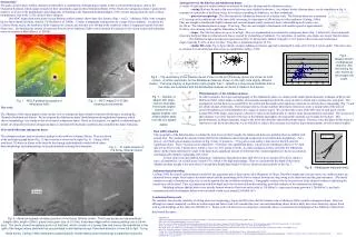
Trench etched Ref.: M. Boufnuchel, P. Lefaucheux, R. Dussart, and P.Ranson, “Dry cryogenic etching of silicon trenches for MEM’s applications”, STMicroelectronics. Trench of 4 um in aperture, 80 um in depth, 1 um undercut, anisotropic with no bowing and etched at 4 um/min ELEC 7730 02'
High aspect ratio line pattern etch • Similar process can be extended to etch trench > 50 um • Results shows excellent center to edge uniformity and smooth sidewall Ref.: Anisul Khan, Ajay Kumar, “High etch rate in silicon and silicon nitride for MEM’s applications”, Applied materials. ELEC 7730 02'
Trench performance on different mask patterns Ref.: Anisul Khan, Ajay Kumar, “High etch rate in silicon and silicon nitride for MEM’s applications”, applied materials. ELEC 7730 02'
Dome and chamber inside surfaces of the DSP deep trench etcher Dome and chamber inside surfaces of the DPS deep trench etcher show no deposition after a 600-wafer continuous marathon. Ref.: Shaoher Pan and Dragan Podlesnik, “A new technology for high-aspect-ratio silicon etch”, Applied materials. ELEC 7730 02'
Conclusion • Can be used for filling deep trenches (50~60um) with oxide without any voids, better quality of trench isolation compared with using LPCVD oxide • Very low temperatures are needed. ( ~ -125°C) • Highly anisotropic holes can be obtained by increasing the temperature ( ~ -105°C). • Aspect ratio rates > 45 • The stability and reproducibility of the process is established by performing process marathon run for more that 60 plasma hours. ELEC 7730 02'
IEP (Interferometric Endpoint) 1. Interferometry is a powerful technique that can be used for endpoint detection of planar layer and trench etching, or deposition. The technique involves illuminating the surface of a sample (typically a wafer) and measuring the reflected intensity. 2. The system may be used as a simple reflectometer, in which case interfaces between materials with different refractive indices can be detected by the resultant step change in the reflectivity signal. Ref.: http://www.jyhoriba.co.uk/jy/tfilms/digilem.htm. ELEC 7730 02'