Download
1 / 10
100 likes | 112 Views
Silicon eyes for radio-labeled biological samples Proposal for the PRIN 2012 call. L. Ratti. Università degli Studi di Pavia, INFN Pavia. PRIN 2009 Collaboration Meeting, Milan, March 28 th 2013. General features of the project. Purpose :

E N D
Silicon eyes for radio-labeled biological samples Proposal for the PRIN 2012 call L. Ratti Università degli Studi di Pavia, INFN Pavia PRIN 2009 Collaboration Meeting, Milan, March 28th 2013
General features of the project Purpose: • develop a semiconductor detection system for (in particular, but not only, 3H) radio-labeled for digital autoradiography of biological specimens • study advanced technological solutions for the design of compact detection systems (sensor array + electronics) featuring high spatial resolution, high functional density and fast readout architecture • develop advanced tools for simulation and test of large detection systems • build a cm-scale demonstrator detector Duration: 3 years ERC Domains: PE (main, 7_2 – Electronic Enginering, and 7_5 – Micro- and Nano-Electronics) and LS (7_2 – Diagnostic Tools)
Participating units UNIBG • Valerio Re (Unit Coordinator) • Massimo Manghisoni • Gianluca Traversi UNINSUBRIA • Massimo Caccia (Unit Coordinator) UNIPV • Lodovico Ratti (PI) • Carla Vacchi The proposal is of the ‘PRIN Advanced’ type
Motivation Present devices for autoradiography (AR) of biological specimens (emulsion films and phosphor imaging plates) feature poor sensitivity and limited dynamic range and linearity and lack the capabilities for real time digital imaging Many feasibility studies and developments based on solid state microelectronic technologies (CCDs, CMOS MAPS, hybrid pixels, DEPFETs) have led to encouraging results, although none of the approaches has demonstrated the capability to satisfy the entire set of requirements for AR (sensitive area, spatial resolution, duty cycle, detection sensitivity) The goal is to demonstrate the feasibility of a large area, high granularity, (almost) zero-dead time, highly sensitive semiconductor detection system for AR by building a (not so) small, seamlessly scalable one
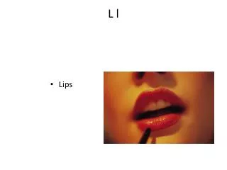
Digital tritium autoradiography Detector specifications: • sensitive area: in tritium AR, single biological samples do not exceed an area of 12 mm x 12 mm; a typical drug discovery experiments is made by some 20 to 40 samples to be imaged simultaneously, therefore requiring quite a large sensitive area; • granularity: between about 20 and 50 μm; a fine pitch would offer the flexibility of optimizing either the image resolution or the contrast depending on the end user specific analysis but, for a given detector area, would increase the power dissipation; • duty cycle: as high as possible to take advantage of the detector sensitivity obtained through sensor and front-end design optimization and noise minimization; due to the very low rate of the source, a sparse readout architecture can be exploited to minimize the data throughput to the DAQ and keep the dead time to a minimum
Digital tritium autoradiography Detector specifications (cont’d): • entrance window: 3.8 keV electrons have a submicron range in silicon; MAPS need to be back thinned to the epitaxial layer, or to 10-20 μm in the case of epiless subtrates; • detection sensitivity to low energy particles: depends on S/N; S is affected by entrance window (<100 nm), CCE and charge sharing, cross talk and impact point position; noise depends on front-end design and detector leakage; target sensitivity is 10-2 decays/minute/mm2; • imaging capability: relies on the detection sensitivity of the sensor and on the ability of the system to reject noise and cosmic ray background hits; • detector mounting: since the detector has to be operated in back illumination conditions, the chip has to be connected to the external bias and I/O circuitry while being bonded face down to the support, in such a way that the chip backside looks toward the radio-labeled samples
Technology choice (likely) The selected microelectronic process is based on a 180 nm CMOS technology with quadruple well option, featuring a relatively thick (up to 18 um) epitaxial layer
Final goal of the project The final product of the project will be a demonstrator consisting in a centimeter-scale detector, exceeding the available commercial and non commercial solutions for autoradiography in resolution and detection sensitivity, together with a data acquisition, processing and visualization system While the fabrication of a real application-scale device is out of the scope of this project, the demonstrator will be designed to be easily expandable to a larger-scale detector
Role of the participating units UNIBG • analog front-end design - choice between CSA+discriminator and 3T readout+CDS, or between binary readout or analog readout+ADC • prototype laboratory tests UNINSUBRIA • prototype characterization with 3H and 14C sources • DAQ development and flltering and imaging algorithm optimization • device qualification with radio-labeled biological samples UNIPV • physics simulation of the collecting electrode - best trade-off among electrode area, geometry and location, and system noise, effects of substrate thinning on the sensor properties, substrate contact distribution • design of a digital architecture with selective readout capabilities – minimum readout bandwidth and maximum duty cycle • prototype laboratory tests
Activity plan The activity program of the project is as follows (mo=month) • mo1 - mo6: design of the first prototype (small area), also based on device simulations for charge collection optimization; investigation and assessment of substrate thinning techniques, chip to PCB flip chip bonding techniques and thin chip support; • mo7 - mo9: first prototype production; setup of the data acquisition based on available laboratory solutions; • mo10 - mo15: first prototype characterization, selection of the best performing architecture; • mo16 - mo23: design of the second, cm-scale prototype; • mo24 - mo26: production of the second prototype; setup of a dedicated data acquisition system; • mo27 - mo36: characterization of the second prototype in laboratory; imaging tests with 3H and 14C standard sources and real radio-labeled biological samples.