Download
1 / 27
290 likes | 639 Views
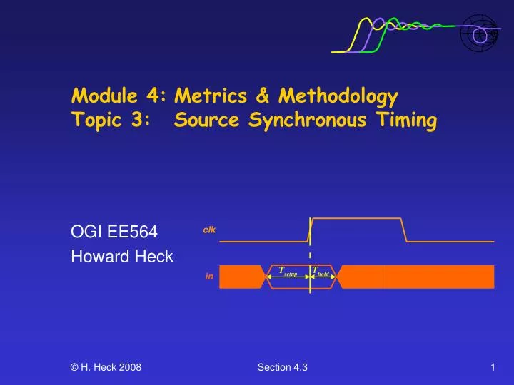
Module 4: Metrics & Methodology Topic 3: Source Synchronous Timing. OGI EE564 Howard Heck. Where Are We? . Introduction Transmission Line Basics Analysis Tools Metrics & Methodology Synchronous Timing Signal Quality Source Synchronous Timing Recovered Clock Timing Design Methodology

E N D
Module 4: Metrics & MethodologyTopic 3: Source Synchronous Timing OGI EE564 Howard Heck Section 4.3
Where Are We? • Introduction • Transmission Line Basics • Analysis Tools • Metrics & Methodology • Synchronous Timing • Signal Quality • Source Synchronous Timing • Recovered Clock Timing • Design Methodology • Advanced Transmission Lines • Multi-Gb/s Signaling • Special Topics Section 4.3
Contents • Synchronous Bus Limitations • Source Synchronous Concept & Advantages • Operation • Timing Equations • Maximum Transfer Rate • Summary • References • Appendix: Timing Equation Derivation Section 4.3
Common Clock Limitations clk • Max frequency is defined by min cycle time • Min cycle time is limited by maximum delays. • Can we find a way to remove the dependence on absolute delays? CLK CLK CORE TO CORE FROM Q Q D D a b Section 4.3
Source Synchronous Signaling Concept • The transmitting agent sends the clock (a.k.a. strobe), along with the data signal. • Overview: • Drive the clock and data signals with a known phase relationship. • Design the clock and data signals to be identical in order to preserve the phase relationship. • As long as the phase relationship can be maintained, the lines can be much longer. Section 4.3
Source Synchronous Concept Example 5.5 ns CLK/CLK# 1.0 ns @ Tx DATA @ Tx 5.7 ns DATA @ Rx 300 ps CLK/CLK# T = 500 ps @ Rx su • Suppose that we transmit a data signal 1 ns prior to transmitting the strobe. • You’re given a 500 ps receiver setup requirement. • You find that the flight time for the data signal varies between 5.5 ns and 5.7 ns. • The flight time for the clock signal also varies between 5.5 ns and 5.7 ns, independent from the data. • Can we meet the setup requirement? Section 4.3
Source Synchronous Advantage • From the preceding example, it should be apparent that source synchronous performance depends on relative, rather than absolute delays. • True for drivers and interconnect, though we must still meet the absolute setup/hold requirements for the receiver. • In real systems, the difference in delay between signals can be made much smaller than the absolute delays. • Therefore, with source synchronous signaling we can expect • to achieve higher performance • to be able to use longer traces Section 4.3
Transfer Rate Comparison Section 4.3
Operation • Typically, there is one strobe signal (or pair of signals) per two bytes of data signals. • Varies by design • Signal relationships at the transmitter are shown below. Section 4.3
Source Synchronous Operation @ RECEIVER Tsumar Thmar Tsu Th STROBE/STROBE Thskew Tsuskew Tvb Tva @ DRIVER DATA t Tsuskew: flight time skew for setup Tsumar: setup margin Tvb: min driver phase offset (setup) Thskew: flight time skew for hold Thmar: hold margin Tva: min driver phase offset (hold) Section 4.3
Source Synchronous Equations @ RECEIVER Tsumar Thmar Tsu Th STROBE/STROBE Thskew Tsuskew Tvb Tva @ DRIVER DATA t The sum of the timings at the receiver must not exceed the phase offsets at the driver: [4.3.1] [4.3.2] the transmitter design requires minimum offsets: [4.3.3] [4.3.4] Section 4.3
Source Synchronous Equations #2 @ RECEIVER Tsumar Thmar Tsu Th STROBE/STROBE Thskew Tsuskew Tvb Tva @ DRIVER DATA t We must also satisfy the following relationship: Tbit: data bit width [4.3.5] This determines our maximum transfer rate. TRmax: max transfer rate [4.3.6] Section 4.3
Question • Based on what we’ve covered in the previous slides, what are the implications to: • The transmitter design? • The receiver design? • The interconnect design? Section 4.3
Example • Tsu = 500 ps, Th = 500 ps • The target transfer rate is 500 MT/s. • What are reasonable flight time skew targets? Section 4.3
Source Synchronous Timing Summary • Synchronous timings are limited by absolute delays. • Source synchronous timings use a strobe eliminate dependence on absolute delay. • Performance depends on our ability to maintain known phase relationship between data & strobe • As a result, source synchronous interfaces typically operate at 2x-8x the clock frequency. • Expect that ratio to scale much higher in the future. • Matching of delays (transmitter & interconnect) is a key design consideration for designing high speed source synchronous interfaces. Section 4.3
References • S. Hall, G. Hall, and J. McCall, High Speed Digital System Design, John Wiley & Sons, Inc. (Wiley Interscience), 2000, 1st edition. • W. Dally and J. Poulton, Digital Systems Engineering, Cambridge University Press, 1998. • R. Poon, Computer Circuits Electrical Design, Prentice Hall, 1st edition, 1995. • H.B.Bakoglu, Circuits, Interconnections, and Packaging for VLSI, Addison Wesley, 1990. • H. Johnson and M. Graham, High Speed Digital Design: A Handbook of Black Magic, PTR Prentice Hall, 1993. • S. Dabral and T. Maloney, Basic ESD and I/O Design, John Wiley and Sons, New York, 1998. Section 4.3
Appendix: Source Synchronous Timing Equation Derivation Section 4.3
Source Synchronous Bus Operation Driver Chip From Core D Q D DELAY Strobe n n From Core D Q P L Data L Clock Distribution Tree Data Receiver Chip To Core Q D Q D System n Clock Strobe P L L Clock Distribution Tree Section 4.3
Operation #2 Driver Chip From Core D Q D DELAY Strobe n n From Core D Q P L Data L Clock Distribution Tree Data Receiver Chip To Core Q D Q D System n Clock Strobe P L L Clock Distribution Tree • The timing path starts at the flip-flop of the transmitting agent and ends at the flip-flop of the receiving agent. • The strobe signal is used as the clock input of the receiver flip-flop. • The transmitted strobe (and data) signals are generated from the on-chip bus clock. • Typically, the strobe is phase shifted by ½ cycle from the data signal. • Duty cycle variations will cause variation on the phase relationship Section 4.3
Setup Timing Diagram & Loop Analysis TBCLK BCLK TBCLK /4 DCLK Tco(STB) DRIVER STB/STB Tco(DATA) Tflight(STB) DRIVER DATA RECEIVER STB/STB Tflight(DATA) Tsu RECEIVER DATA Tsumar t [4.3.1a] Section 4.3
Setup Analysis [4.3.1a] [4.3.2a] [4.3.3a] • For a “double pumped” bus, the difference between Tco(DATA) and Tco(STB) is typically set to one-half of the cycle time (TDCLK/2 = TBCLK/4) to center the strobe in the data valid window. • Double pumped: source synchronous transfer rate is 2x the central clock rate. • This relationship is typically specified as Tvb (data “valid before” strobe ), which signifies the minimum time for which the data at the transmitter is valid prior to transmission of the strobe. • Mathematically: • Simplify the loop equation: Section 4.3
Setup Analysis #2 [4.3.4a] [4.3.5a] [4.3.6a] • Both data & strobe propagate over the interconnect. • Goal: identical flight times. • In reality, there will be some difference in flight times between data and strobe. • trace length, loading, crosstalk, ISI, etc. • Define flight time skew for the setup condition: • Simplify the loop equation: Section 4.3
Notes on the Setup Equation [4.3.7a] • You may see the timing equation written in other forms. • The way I defined Tvb makes it a negative quantity. Others may define it to be positive. • I defined Tsuskew to be a positive quantity. Section 4.3
Hold Timing Diagram & Loop Analysis TBCLK BCLK TBCLK/4 DCLK Tco(STB) Tco(DATA) DRIVER STB/STB Tflight(STB) DRIVER DATA Th RECEIVER STB/STB Tflight(DATA) Thmar RECEIVER DATA t Section 4.3
Hold Analysis [4.3.9a] [4.3.10a] [4.3.11a] • Just as for the setup case, we need to specify the minimum phase relationship between data and strobe: [4.3.8a] • In addition, define the flight time skew for the hold case: • In addition, define the flight time skew for the hold case: • Note that the Thskew is defined such that it is a negative quantity, while Tva is defined to be positive. Section 4.3
Maximum Transfer Rate -T T vb,min va,min STB/STB DATA T cycle,min • The maximum transfer rate can be determined using the definitions for Tva and Tvb. • We can calculate the limit of TBCLK (for a double pumped bus) by adding the two equations above. [4.3.12a] Section 4.3
Higher Transfer Rates (e.g. “Quad Pumped”) • The setup and hold equations remain the same. • What changes are the Tva and Tvb definitions: [4.3.13a] [4.3.14a] Section 4.3