Download
1 / 33
330 likes | 719 Views
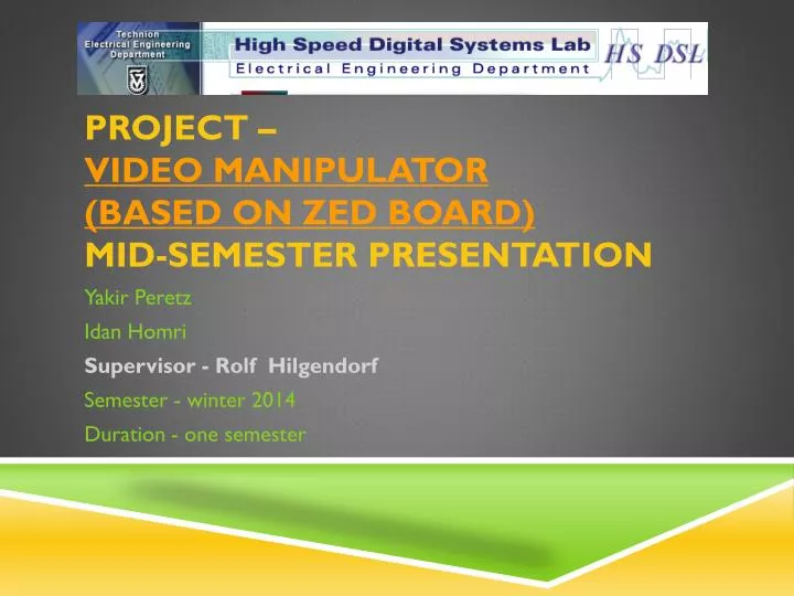
Project – Video manipulator (based on Zed Board) mid-semester presentation. Yakir P eretz Idan Homri Supervisor - Rolf Hilgendorf Semester - winter 2014 Duration - one semester. agenda. Project goals Component description Data flow Required tests and check points Clock definitions

E N D
Project – Video manipulator(based on Zed Board)mid-semester presentation YakirPeretz IdanHomri Supervisor - Rolf Hilgendorf Semester - winter 2014 Duration - one semester
agenda • Project goals • Component description • Data flow • Required tests and check points • Clock definitions • Software description • Critical issues and solutions • Complete Program (without Uart)
Project goals • Creating a system that enables reading images from an external device, saving it in the memory and displaying it by RGB. • Creating a programmable logic design that will handle the transportation of the data from the main memory to the VGA output via video direct mapped accessed (VDMA) component. agenda
Component description -ZYNQ • In the design we use the following components: • ZYNQ processor • the ZYNQ is actually the PS part of the design, which means all the software programmable part. • This part is very powerful and includes many features, but we use the following: • UART connection • memory controller • the memory itself - DDR3 • One ARM processor–CORTEX A9 • All the needed interface connections to the other components in the PL side are built in. • All the clocks of the design are generated by the zynq, and given to the relevant components. • PS side overview
Component description -VDMA • VDMA • The VDMA is the core of the PL side of the design. It is responsible for the transportation of the data from the memory to the stream part. It is connected to three other components via three buses: • To the processor via AXI4-lite – to get data regarding the address and size of the data to get from the memory. • To the memory controller via full AXI4 – to get the data from. • To the “stream_to_video_out” via AXI4-stream – to send the data to. • the data transportation to the stream part is done with respect to the VTC timing signals. • VDMA
Component description - VTC • Video timing controller • this component is responsible for timing the data transfer from the VDMA to the stream to video out component. • It generated signals regarding the vertical data transfer (line count) and the horizontal data transfer (pixels per line) as well as the active video signal. • It works with a clock that is set in order to fit the data size and rate of pictures per second - Clock definitions • Video timing controller
Component description - stream • Stream to video out – AXI4-Stream to Video Out core converts AXI4-Stream Video protocol from Xilinx video processing cores such as VDMA, that use this protocol, to video output with explicit sync and timing such as the unit we built to communicate with the VGA port. • In our project, the unit is used to convert the output of the VDMA in AXI_stream protocol to an actual video protocol that consists of: • Active data signal • Vertical sync and horizontal sync • Blank periods • “Stream to video out” interface
Component description – RGB_out • RGB_out • this unit was built by us, to convert the data from 8 bit per color (for red green and blue) to 4 bit per color. • The output of this unit is the input of the VGA ports • RGB – 4 bits per color • Vsync • Hsync. agenda RGB_out
Data flow agenda
Required tests and check points • We have some strategic check points for validating our design: • Uart to memory – we first check that the data we delivered from an external device true the Uartis saved in the memory where we wanted it to be saved. • Memory to VDMA – we check that the data is transferred correctly from the memory to the frame bufers inside the VDMA. • VDMA to “stream_to_video_out”– we check that the data is transferred correctly from the VDMA to the stream to video out by reading the data runs on the AXI_stream bus. • Control signals – we need to check that the “video_timing_controller” is sending the timing signals as we assumed it will. • “stream_to_video_out” to VGA – we check if the data from the “stream_to_video_out” is sent as we wanted in a 24 bit (8 bit per color and 3 colors R,G,B) format. • VGA output – we need to check that the data in the output of the VGA component is the picture we delivered. This should be displayed on the screen. • Block Diagram agenda
Clock definitions • There are 2 main clocks in the design (beside the ARM clock & DDR clock) • The faster clock is used for the AXI4_lite bus that connects the ARM and the VDMA. On that bus the ARM transfers the data regarding the address and the size of the picture in the memory. the clock is set to 200MHZ • The slower clock is used for the full AXI4 bus and the AXI_stream bus. On that bus we move the data from the memory to the VDMA and then from the VDMA to the “stream to video out” unit. • That clock is defined to be 148.5 mega pixels per second. That is calculated to fit the amount of data being transferred in one second, calculated as: • (number of lines including blank)*(number of pixels per line including blank)*(number of pictures per second) – for us - 2200*1125*60 = 148.5[MHz] • In order to fit to the screen in the lab we needed a 1080*1920, and there are 60 pictures per second. (the sizes represent pixels). agenda Component description - VTC
Block Diagram VDMA sub system ZYNQ sub system Data flow Required tests and check points
PS side overview To VDMA via Axi lite Data flow To VDMA via AXI-4 Component description -ZYNQ
“Stream to video out” interface From VDMA To RGB out From video timing controller Component description - stream Data flow
Video timing controller For write channel – Not in use Optionally – can be controlled by the processor. Not in use Output timing signals for the stream_to_video_out unit Component description - VTC Data flow
RGB_out Data – 4 bits per color Input Sync signals Output Sync signals Data – 8 bit per color Component description – RGB_out Data flow
VDMA Connected to memory on a full AXI4 bus. Required for data transfer This is the connection to the processor. It Transports data regarding the address and the size of the picture Connected to STVO on an AXI4 stream bus. Required for data transfer Data flow Those are the 3 clocks of the design Component description -VDMA
Software Flowchart Host - Matlab Rescaling of BMP Image, open Uart for writing and sending the Image. ZedBoard –C codeSDK Image initialization – White image Vdma Configuration and Setup Vdma Start Transfer Load the incoming Image from Uart into DDR. Start transmission of new Image. agenda
APPENDIX SOFTWARE
Matlab • The main goal of the program is to create Matlab GUI interface between the PC and Zedboard in order to load the desired image. • Step One: Determine the desired uart port configuration. (8 data bit, 1 stop bit, 115200 baud rate) • Step two: Load the bitmap image into Matlab and make dimensions’ rescale: 640 * 480 or 1080 * 1920 • Step Three: Open the port and send information • Step Four: For Testing Purpose Only- read back the Image and display on screen software flowchart
C code – SDKLoad Picture into DDR • Program should read the incoming data and load it into the DDR. At this point of the Project we encounter a technical problem – Zedboard buffer size at polling mode is 65 bytes only, so there is no option at this time to load the whole picture. • In order to continue with the development, the pictures were written manually into the DDR. software flowchart
Problem – “Works” Only in Remote mode. Matlab is sending and receiving by itself. No data is written into Zed board Buffer. This can indicate that Matlab transportation data is fine, but zedboard reading is not. Other uart modes (as Local Loop for exp) get only first 65 Bytes. software flow
C code – SDKVdma Configuration and Setup • Initialize DMA engine – A VDMA instance is set to VDMA Physical address • Setup the Read channel- The VDMA module use only Read Channel (mm2s). Setup of vertical and horizontal lengths, frames store start address, and other unused Registers. software flowchart
C code – SDKVdma Start Transfer • Start the DMA engine to transfer – the VDMA read channel is activated. • parking on a frame –The vdma reads the same image, in order to display image on screen Continuously. • The VDMA jumps between two images using a counter. It performs temporary parking for each image. software flowchart
Solution – disable caches Critical issues and solutions
VDMA sub system Block Diagram
ZYNQ sub system Block Diagram