Download
1 / 2
30 likes | 171 Views
Tailoring the Properties of Dilute Nitride- Bismide Semiconductor Alloys Rachel Goldman, University of Michigan Ann Arbor, DMR 1006835.

E N D
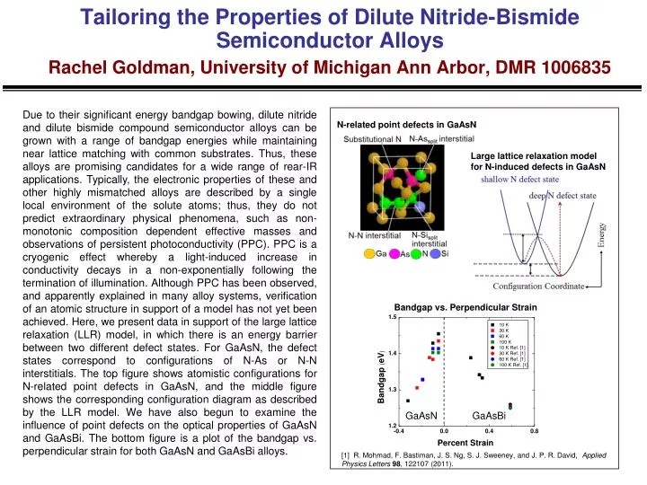
Tailoring the Properties of Dilute Nitride-Bismide Semiconductor AlloysRachel Goldman, University of Michigan Ann Arbor, DMR 1006835 Due to their significant energy bandgap bowing, dilute nitride and dilute bismide compound semiconductor alloys can be grown with a range of bandgap energies while maintaining near lattice matching with common substrates. Thus, these alloys are promising candidates for a wide range of rear-IR applications. Typically, the electronic properties of these and other highly mismatched alloys are described by a single local environment of the solute atoms; thus, they do not predict extraordinary physical phenomena, such as non-monotonic composition dependent effective masses and observations of persistent photoconductivity (PPC). PPC is a cryogenic effect whereby a light-induced increase in conductivity decays in a non-exponentially following the termination of illumination. Although PPC has been observed, and apparently explained in many alloy systems, verification of an atomic structure in support of a model has not yet been achieved. Here, we present data in support of the large lattice relaxation (LLR) model, in which there is an energy barrier between two different defect states. For GaAsN, the defect states correspond to configurations of N-As or N-N interstitials. The top figure shows atomistic configurations for N-related point defects in GaAsN, and the middle figure shows the corresponding configuration diagram as described by the LLR model. We have also begun to examine the influence of point defects on the optical properties of GaAsN and GaAsBi. The bottom figure is a plot of the bandgap vs. perpendicular strain for both GaAsN and GaAsBi alloys. N-related point defects in GaAsN Large lattice relaxation model for N-induced defects in GaAsN Bandgap vs. Perpendicular Strain GaAsN GaAsBi [1] R. Mohmad, F. Bastiman, J. S. Ng, S. J. Sweeney, and J. P. R. David, Applied Physics Letters98, 122107 (2011).
Undergraduate and High School Students in ResearchRachel Goldman, University of Michigan Ann Arbor, DMR 1006835 Participation in research is a proven way to enhance the quality of education and encourage students to pursue STEM careers. To date, this project has provided research training for a total of 4 graduate and 4 undergraduate students. All of the students learned about semiconducting materials and their importance for electronic and photonic applications while participating in their projects. In addition, the students learned a combination of various technical skills such as ultra-high vacuum techniques, molecular beam epitaxy, and electron transport measurements. For the past five years, we have solicited substantial involvement of local high school students in research. Many students have been successful in local and regional science fair competitions. We are currently endeavoring to expand the program to involve students and teachers from other local high schools. The PI had several planning meetings with the Superintendent of the Ann Arbor schools and is in the process of solidifying arrangements. Undergraduates Sarah Paleg (top) with the molecular beam epitaxy system and Charlie Gorman (bottom) taking X-ray diffraction measurements.