Download
1 / 4

E N D
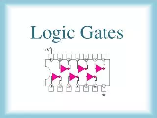
Most of today’s SSIs are cased in DIPs, or dual-in-line packages. Each pin corresponds to a number, with pin number 1 can be as found in the drawing. This part of the IC is indicated by the half crescent found on the IC, or by just looking at the IC label, where pin no.1 is found on the lower left as shown. The numbering of the pins are also shown, following a U-shaped pattern.
Each boolean function in the IC corresponds to a code number. Usually for TTL or Transistor-Transistor Logic Integrated Circuits, the SSIs have such code names as 7404s for inverters, 7408s for AND gates and 7432s for OR Gates
Single-input SSIs in Dual-In-Line Packages • In this package there are six logic gates in each DIP +Vcc A6 Y6 A5 Y5 A4 Y4 14 13 12 11 10 9 8 • The number 1 to 14 are called pin number • Adenotes input of logic gate i • Y denotes output of logic gate i. 1 2 3 4 5 6 7 A1 Y1 A2 Y2 A3 Y3 Vss