Download
1 / 37
370 likes | 380 Views
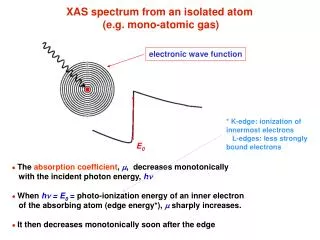
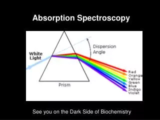
L4 092016 ECE 4243/6243 Fall 2016 UConn F. Jain Notes Chapter L6 (page 105-128). Optical transitions in quantum confined systems. 1.Photon absorption involves electronic transitions:

E N D
L4 092016 ECE 4243/6243 Fall 2016 UConn F. Jain Notes Chapter L6 (page 105-128). Optical transitions in quantum confined systems 1.Photon absorption involves electronic transitions: -Valence band-to-conduction band, acceptor impurity band or levels to conduction band, donor levels/band-to-acceptor levels, and intra-band or free carrier transitions (within conduction or valence band). -Absorption is dependent on probability of a transition and density of states in valence and conduction bands. Probability depends if it is direct gap or indirect. In indirect semiconductors, phonon participation is essential to conserve momentum. -Density of states depend on the physical structure of the absorbing layer if it is thick (>10-15nm), or thin (~5-10nm). In terms of thin layer, we need to know if it comprise of quantum wells, quantum wires, and quantum dots. -Generally, absorption starts when photon energy is about the band gap. It increases as hn increases above the band gap Eg. In the case hn <Eg, excitonic transitions can take place. Their range is very narrow as exciton binding energy is 0.004-0.012 eV. -In general absorption coefficient in quantum wires is higher than in wells. It also starts at higher energy than band gap in bulk materials due to quantum confinement.
Absorption and emission of photons 1) (Transition Probability) here, (h) is the joint density of states in a volume V (the number of energy levels separated by an energy Fig. 2 absorption as a funciton of photon energy. 2) Pmo probability that a transition has occurred from an initial state ‘0’ to a final state ‘m’ after a radiation of intensity I(h) is ON for the duration t. The joint density of states is expressed as Eq. 2B) o
2.Photon emission involves downward transitions: Downward transitions are classified as radiative and non-radiative. When photon is not emitted, it is non-radiative. -Band-to-band transitions could involve free carriers or excitonic transitions. Rate of emission in quantum wells is higher than in bulk layers. Rate of emission in quantum wires is higher than in quantum wells. Rate of emission in quantum dots is higher than in quantum wires. Rate of emission has two components: Spontaneous rate of emission Stimulated rate of emission. Absorption coefficient is related to rate of emission using Van Roosbroeck- Shockley. This enables obtaining an expression for radiative transition lifetime tr. There are ways to compute non-radiative lifetime tnr. The internal quantum efficiency is expressed as follows: Pr is the probability of a radiative transition.
·Direct and Indirect Energy Gap Semiconductors (p.106) Semiconductors are direct energy gap or indirect gap. Metals do have not energy gaps. Insulators have above 4.0eV energy gap. Fig. 10b. Energy-wavevector (E-k) diagrams for indirect and direct semiconductors. Here, wavevector k represents momentum of the particle (electron in the conduction band and holes in the valence band). Actually momentum is = (h/2p)k = k
Effect of strain on band gap (page 106) Ref: W. Huang, 1995 UConn doctoral thesis with F. Jain • Under the tensile strain, the light hole band is lifted above the heavy hole, resulting in a smaller band gap. • Under a compressive strain the light hole is pushed away from heavy. As a result the effective band gap as well as light and heavy hole m asses are a function of lattice strain. Generally, the strain is +/- 0.5-1.5%. "+" for tensile and "-" for compressive. • Strain does not change the nature of the band gap. That is, direct band gap materials remain direct gap and the indirect gap remain indirect.
Electrons & Holes Photons Phonons Statistics Fermi-Dirac & Maxwell-Boltzmann (classical) Bose-Einstein Bose-Einstein Velocity vth ,vn 1/2 mvth2 =3/2 kT Light c or v = c/nr nr= index of refraction Sound vs = 2,865 meters/s in GaAs Effective Mass mn , mp (material dependent) No mass No mass Energy E-k diagram Eelec=25meV to 1.5eV ω-k diagram (E=hω) ω~1015 /s at E~1eV Ephotons = 1-3eV ω-k diagram (E= ω) ω~5x10¹³/s at E~30meV Ephonons = 20-200 meV Momentum P= k k=2π/λ λ=2πvelec/ω momentum: 1000 times smaller than phonons and electrons P= k k=2π/λ λ=2πvs/ω
Absorption coefficient and rate of emission and complex index of refraction Index of refraction nc is complex when there are losses. nc= nr – i k where extinction coefficient k = α/4pn, here alpha is the absorption coefficient. Also, nc is related to the dielectric constant. nc = =
Mathematical Representation of QCSE Under Electric Field, Excitonic binding energies decrease Fig 20. Refractive index of 5nm QD with 50kV/cm and 100kV/cm E field.
Absorption coefficient is related to rate of emission. Absorption coefficient is related to imaginary component of the complex index of refraction. Eq. 7 –page 214-ECE5212 is the rate of emission of photons at within an interval Van Roosbroeck - Shockley Relation under equilibrium Eq. 8 –page 214 Index of refraction nc is complex when there are losses. nc= nr – i k where extinction coefficient k = α/4pn, here alpha is the absorption coefficient. Also, nc is related to the dielectric constant. nc = = In non-equilibrium, we have excess electron-hole pairs. Their recombination gives emission of photons. The non-equilibrium rate of recombination Rc is In equilibrium,
Radiative life time in intrinsic and p-doped semiconductors (p.216) Nonradiative recombination: Auger Effect and other mechanisms (217) Nonradiative transitions are processes in which there are no photons emitted. Thus, there are several models by which energy is dissipated. Experimental observations are in terms of (1) emission efficiency, (2) carrier lifetime (coupled with emission kinetics), (3) behavior (or recombination mechanisms response) to temperature and carrier concentration variations. Recombination processes which are not associated with an emission of a photon are as follows: • Auger effect (carrier-carrier interaction) • Surface recombination, recombination through defects (Shah-Noyce-Shockley) • Multi phonon emission and others which may fit with the above proposed criterion. Since Auger processes involve carrier-carrier interactions, it is typical to assume that probability of occurrence of such a process should increase with the carrier concentrations.
e e First term: AnP Second Term: Bp2 h h Auger Transitions: Nonradiative (n type semiconductor) (p type semiconductor)
Spectral width of emitted radiation Density of states in bulk is N(E)dE = The electron concentration ‘n’ in the entire conduction band is given by (EC is the band edge) This equation assumes that the bottom of the conduction band is =0. Electron and hole concentration as a function of energy
Graphical method to find carrier concentration in bulk or thick film (Chapter 2 ECE 4211)
Graphical method to find carrier concentration in quantum well Spectral width in quantum well active layer is smaller than bulk thin film active layer. See how to solve for Fermi level from charge neutrality condition.
DEVICES based on optical transitionsEmission: LEDs and LasersAbsorption: Solar cells, PhotodetectorsOptical modulators using electro-absorption or electro-refractionOptical switchesandOptical logic (Self electro-optic devices or SEED Devices p.172)
Eg Ehh1 Fig. 1(a) E = 0 Quantum confined Stark Effect (page 169, L9) Electro-absorption and electro-refraction and their application as Optical Modulators We cover basics of exciton formation in quantum wells and related changes in the absorption coefficient and index of refraction. This phenomena is called confined Stark effect. Photon energy needed to create an exciton is given by h = Eg + (Ee1 + Ehh1) - Eex (Bulk Band gap) (Zero field energy of (Binding energy Electron and holes) of exciton) If the photon energy is greater than above equation, free electron and hole pair is created. Ee1
Electron wave function Hole wave function Fig. 1(b) Quantum well in the presence of E Application of perpendicular Electric Field When a perpendicular electric field is applied, the potential well tilts. Its slope is related to the electric field. • As E increases Ee & Eh decreases. As a result photon energy at which absorption peak occurs shifts to lower values (Red shift) . • The interaction between electron and hole wavefunctions (and thus, the value of the optical matrix elements and absorption coefficeint) also is reduced as magnitude E is increased. This is due to the fact that electron, hole wave functions are displaced with respect to each other. Therefore, the magnitude of absorption coefficient decreases with increasing electronic filed E.
MQW Modulator based on change in absorption due to quantum confined Stark effect Fig.3. Responsivity of a MQW diode (acting as a photodetector or optical modulator).
Quantum Confined Stark Effect (QCSE) in Conventional Field Effect Structure (FES) • Quantum Confined Stark Effect: • Under electric fields, large shifts in optical absorption and change in refractive index are observed. • Result of decreases wave function interaction. (electron states to lower energies, holes to higher energies) Fig 17. Resulting absorption shift via QCSE.[6] Fig 18. (a) refractive index increase (higher absorption) in MQW. (b) Refractive index shift increases.
QD Modulator Modeling • Modeling of II-VI (ZnSe-CdSe) QDs • Electro-Absorption • Greater binding energies = more stable excitons (smaller QD advantageous) • Electro refraction • Index changes occur singular for large QDs • Previously modeled index changes up to .021 Fig 18. Absorption change of 30Å QDs under varying field.[13] • Modeling Hierarchy • Calculation of elastic Strain in the superlattice (mismatch) and calculate new band gap and band offset. • Create Hamiltonian to solve Schrodinger's equation for wavefunction. • Calculate imaginary part of dielectric constant (exciton transitions included) • Calculate real part of the dielectric constant using Kramer-Kronig relations • Calculate index of refraction and absorption coefficients. [13] Fig 19. Refractive index change of 30Å QDs for varying bias Voltages. [13]
Phase Modulator: A light beam signal (pulse) undergoes a phase change as it transfers an electro-optic medium of length ‘L’ --------------- (1) In linear electro-optic medium …………………(2) E= Electric field of the RF driver; E=V/d, V=voltage and d thickness of the layer. r= linear electro-optic coefficient n= index
Figure compares linear and quadratic variation Dn as a funciton of field. MQWs have quadratic electro-refractive effect. Figure shows a Fabry-Perot Cavity which comprises of MQWs whose index can be tuned (Dn) as a funciton of field.
Mach-Zehnder Modulator Here an optical beam is split into two using a Y-junction or a 3dB coupler. The two equal beams having ½ Iin optical power. If one of the beam undergoes a phase change , and subsequently recombine. The output Io is related as Mach-Zehnder Modulator comprises of two waveguides which are fed by one common source at the input (left side). When the phase shift is 180, the out put is zero. Hence, the applied RF voltage across the waveguide modulates the input light.
Quantum Dot Optical Modulator Design Criteria (J. Khan, UCONN PhD Prospectus) • Design Criteria • Single mode propagation at appropriate wavelength • Wave guiding taper (MFD matching) to fiber • Maximum QD effective area along ridge (ridge height reduction, 32nm QD layer) • High-density integrated optical waveguides, a high-index contrast is mandatory • Si index of refraction 3.44 • SiO2 has index of refraction of 1.97 • Si/SiO2 ridge waveguide offers large index of refraction delta of 43% 10um 15um .3um Fig 26. Cross Section view of integrated ridge waveguide.[3] Fig 25. Cross Section view of integrated ridge waveguide.[17]
Why quantum well, wire and dot lasers, modulators and solar cells? Quantum Dot Lasers: • Low threshold current density and improved modulation rate. • Temperature insensitive threshold current density in quantum dot lasers. Quantum Dot Modulators: • High field dependent Absorption coefficient (α ~160,000 cm-1) : Ultra-compact intensity modulator • Large electric field-dependent index of refraction change (Δn/n~ 0.1-0.2): Phase or Mach-Zhender Modulators Radiative lifetime τr ~ 14.5 fs (a significant reduction from 100-200fs). Quantum Dot Solar Cells: High absorption coefficent enables very thin films as absorbers. Excitonic effects require use of pseudomorphic cladded nanocrystals (quantum dots ZnCdSe-ZnMgSSe, InGaN-AlGaN) Table I Computed threshold current density (Jth) as a function of dot size infor InGaN/AlGaN Quantum Dot Lasers (p.11) (Ref. F. Jan and W. Huang, J. Appl. Phys. 85, pp. 2706-2712, March 1999).
Transitions in Quantum Wires: The probability of transition Pmo from an energy state "0" to an energy state m in the conduction band "m" is given by an expression (derived in ECE 5212). This is related to the absorption coefficient a as shown in slide 2. It depends on the nature of the transition. The gain coefficient g for stimulated emission depends on the absorption coefficient aas: g = -a(1- fe - fh ). The gain coefficient g can be expressed in terms of absorption coefficient a, and Fermi-Dirac distribution functions fe and fh for electrons and holes, respectively. Here, fe is the probability of finding an electron at the upper level and fh is the probability of finding a hole at the lower level. Free carrier transitions: A typical expression for g in semiconducting quantum wires, involving free electrons and free holes, is given by:
Excitonic Transitions in Quantum Wires: gain coefficient Excitonic Transitions: This gets modified when the exciton binding energy in a system is rather large as compared to phonon energies (~kT). In the case of excitonic transitions, the gain coefficient is:
In the case of lasers, we need to find the gain coefficient and its relationship with fe and fh, which in turn are dependent on the current density (injection laser) or excitation level of the optical pump (optically pumped lasers). The gain coefficient depends on the current density as well as losses in the cavity or distributed feedback structure. Threshold current density is obtained once we substitute g from the above equation. For modulators, we need to know: • Absorption and its dependence on electric field (for electro-absorptive modulators) • Index of refraction nr and its variation Dn as a function of electric field (electro-refractive modulators) • Change of the direction of polarization, in the case of birefringent modulators. In the presence of absorption, the dielectric constant e (e1-je2) and index of refraction n (nr –j k) are complex. However, their real and imaginary parts are related via Kramer Kronig's relation. See more in the write-up for Stark Effect Modulators.
p114 notes 4. Quasi Fermi Levels Efn, Efp, and Dz Quantum Wells Quantum Wires Quantum Dots
Laser operating wavelength (p 114) 5. Operating Wavelength l: The operating wavelength of the laser is determined by resonance condition L=ml/2nr Since many modes generally satisfy this condition, the wavelength for the dominant mode is obtained by determining which gives the maximum value of the value of the gain. In addition, the index of refraction, nr, of the active layer is dependent on the carrier concentration, and knowing its dependence on the current density or gain is important. For this we need to write the continuity equation. 6. Continuity equation and dependence of index of refraction on injected carrier concentration The rate of increase in the carrier concentration in the active layer due to forward current density J can be expressed as: