Download
1 / 43
440 likes | 461 Views
Statements on Societal Implications. Rational You ITRI-IEK-NEMS 2001/08/16. Source: NSF (2001/03). S-Curve of Technology. The concept of an S-curve of technology Present position on the S-curve of technology. Source: NSF (2001/03). A Secure Nation in a Secure World. ---.

E N D
Statements on Societal Implications Rational You ITRI-IEK-NEMS 2001/08/16 Source: NSF (2001/03)
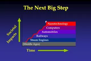
S-Curve of Technology • The concept of an S-curve of technology • Present position on the S-curve of technology Source: NSF (2001/03)
A Secure Nation in a Secure World • --- Source: NSF (2001/03)
Open System Biosphere • A city model for sustainable energy, agriculture, and climate. Source: NSF (2001/03)
Creating Small, Smart Swarms of Devices • Nanotechnology may be a Key Enabling Element to Creating Small, Smart Swarms of Devices that sense, think, act, and communicate — resulting in emergent behavior of collective systems. Source: NSF (2001/03)
Disruptive Technologies • Nanotechnology may fall into the category of disruptive technologies where significant new capabilities and industrial systems bring large-scale changes, which may result in the betterment of society or may create new problems. Source: NSF (2001/03)
A computer integrates structure and function on many length scales. • A transistor includes some layers of differentiated materials only a few atoms thick. • However, our ability to impart structure at scales less than 180 nm is limited. • In contrast, biological systems are richly structured all the way to the atomic scale. Source: NSF (2001/03)
A recent example from IBM Research (a) Careful control and steering of process conditions can produce technologically useful structures on several length scales. • Here chemical synthesis of uniformly sized nanocrystals and subsequent deposition of the particles from liquid solution forms a nanocrystal superlattice. (b) Comparison of current “state-of-the-art” magnetic storage medium with a nanostructured magnetic storage medium. • Such nanostructured materials may contribute to cost-performance improvements in hard disk drives in the next few years. Source: IBM (Sun et al. 2000), NSF (2001/03)
Electronic Devices using Organic Molecules A world-wide community of researchers is currently pursuing the dream of printing or stamping electronic devices using organic molecules chosen to take advantage of natural assembly processes. (a) Transistors fabricated from the organic semiconductor pentacene exhibit performance comparable to the amorphous silicon transistors used in flat panel displays. (Dimitrakopoulos et al. 1999) (b) Yellow light from a diode made from a hybrid organic-inorganic compound, which was crystallized at room temperature from liquid solution (Chondroudis and Mitzi 1999). Source: NSF (2001/03)
Societal Impact of IC “Scaling” via Pervasive, Affordable Electronics • Economic Growth – Development of “High-Tech” Industries and Workforce – High-Productivity Economy • Personal Equality/Opportunity – Global/Portable Communications – Personal Access to Vast Information On-Demand (News, Education, Entertainment) – Empowerment of Individuals to Process Information (Networked PCs and PDAs vs. Mainframe Computers) Source: NSF (2001/03)
Manufacturing Cost Projection (for Logic at silicon-area and transistor levels) Source: NSF (2001/03)
Smaller Features Lower Cost/Function Larger market • --- Source: NSF (2001/03)
How to Manufacture Nano-Electronic ICs In the future, how do we cost effectively manufacture “almost atomically-perfect” Nano-Electronic ICs ? (based on silicon, nanotubes, or whatever) 1. Nano-Tool Arrays ? – Multiple-Tip AFM lithography ? 2. Self-Assembly ? (perhaps DNA + Enzymes !) – Processing in a low-cost “beaker” ? – “Defect immunity” and/or self repair ? Source: NSF (2001/03)
Suggested Guiding Principles for Long-Range Nanotechnology Research ‧Start Early! ‧Maximize Inter-disciplinary Collaboration ‧Use/Extend the ITRS as a Consensus-Building Forum on“Long-Range Research Needs” for Nanoelectronics ‧Encourage Broad Cooperation ‧Involve Industry as Stakeholders/Customers ‧Utilize University Research Capability ‧Leverage Federal/National Laboratories ‧Emphasize Pre-competitive Results (e.g., not proprietary) ‧Include Studies on Technology Choices/Down-Selection and Technology Migration/Displacement Source: Texas Instruments (R. Doering), NSF (2001/03)
Internet/Comm. driving IC demand to the next level • --- Source: NSF (2001/03)
Approaching a “Red Brick Wall?” Challenges/Opportunities for Semi R&D • --- Source: NSF (2001/03)
Is Lg @ 25 nm the CMOS Limit? • --- Source: IBM, (Wong, Frank, and Solomon 1998 IEDM), NSF (2001/03)
Shipments of U.S. Pharmaceutical Products • --- Source: NSF (2001/03), McConnell (1998)
Technologies — Bio, Info and Nano • The first is “tele-presence.” • The second is health care. • The third is conversing with our machines. Source: NSF (2001/03)
Quantum Phenomena (a) Scanning tunneling micrograph of a square Fe atom corral on a Cu substrate. (b)Fluorescence emission spectra of semiconductor nanoparticles of different sizes and composition (red = InAs (2.8-6.0 nm dia.), green = InP (3.0-4.6 nm), blue = CdSe (2.1-3.6 nm)). ‧The inset shows a set of different-sized, fluorescing CdSe particles in aqueous solution excited by a single UC source. Source: NSF (2001/03)
The Science of Large Numbers of Objects • FePt colloidal particles • a CdSe tetrapod Source: NSF (2001/03)
Colloidal crystal of 100 nm polystyrene spheres • --- Source: NSF (2001/03)
Applications of liquid and supercritical CO2 (1) • Challenges in Nano-scale Device Fabrication—Capillary Forces of Process Solvents Destroy! Source: NSF (2001/03)
Applications of liquid and supercritical CO2 (2) • Defect Density of Microelectronics vs Film Thickness Source: NSF (2001/03)
Applications of liquid and supercritical CO2 (3) • Capillary forces of manufacturing/processing solvents are more challenging as structures become smaller • Surface tension and viscosity of CO2 are more “gas-like” than “liquid-like” • Environmentally sustainable Source: NSF (2001/03)
NanoManipulator interface • --- Source: NSF (2001/03)
Nano-publication Database: SPRU Main Fields • --- Source: NSF (2001/03)
Nano-publication Database: SPRU Sub-Fields • --- Source: NSF (2001/03)
Distribution of Nano-Patents (Over Time and by Technological Fields Period filed) • --- Source: NSF (2001/03)
The different data sets and their overlap • --- Source: NSF (2001/03)
Patent Citations By Organizational Categories (1) • --- Source: NSF (2001/03)
Patent Citations By Organizational Categories (2) By Other Machinery • --- Source: NSF (2001/03)
Patent Citations By Organizational Categories (3) Metal Products, e.g., Machines • --- Source: NSF (2001/03)
Patent Citations By Organizational Categories (4)Electronics • --- Source: NSF (2001/03)
-- • --- Source: NSF (2001/03)
Search Terms Used by Braun et al. Source: NSF (2001/03)
Patent citations and their context • --- Source: NSF (2001/03)
Distribution of Papers by Major Field by SPRU Classification • --- Source: NSF (2001/03)
The Subfield Distribution of Nano-Papers by SPRU-Classification (1) • --- Source: NSF (2001/03)
The Subfield Distribution of Nano-Papers by SPRU-Classification (2) • --- Source: NSF (2001/03)
Early electric car • --- Source: NSF (2001/03)
Polymer rods embedded (with cadmium selenide nanocrystals, fluorescing at various wavelengths) • --- Source: NSF (2001/03)
Two Representations of Quantum Confinement • --- Source: NSF (2001/03)