Download
1 / 24
260 likes | 352 Views
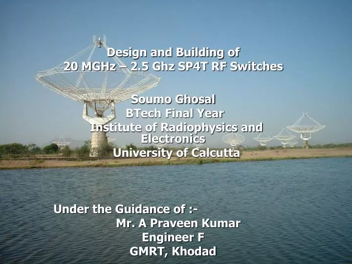
Design and Building of 20 MGHz – 2.5 Ghz SP4T RF Switches Soumo Ghosal BTech Final Year Institute of Radiophysics and Electronics University of Calcutta Under the Guidance of :- Mr. A Praveen Kumar Engineer F GMRT, Khodad. RF/ Microwave Switches.

E N D
Design and Building of 20 MGHz – 2.5 Ghz SP4T RF Switches Soumo Ghosal BTech Final Year Institute of Radiophysics and Electronics University of Calcutta Under the Guidance of :- Mr. A Praveen Kumar Engineer F GMRT, Khodad
RF/ Microwave Switches • Switching is one of the most important function in control of microwave signals • Microwave switch is a microwave circuit made up of high speed microwave devices. • PIN diodes , GaAsFET MMIC are used extensively. • The GMRT Receiver System also puts to use microwave switches at various stages such as : (1) Band Selection (2) Swicthing Filter Banks (3) Attenuator Selection (4) Injection of various levels of noise for calibrating the receiver system 13/11/07 soumoghosal@gmail.com2
Switch Design Configurations • Series Series SPST 13/11/07 soumoghosal@gmail.com3
(2) Shunt : 13/11/07 soumoghosal@gmail.com4
(3)Series Shunt : 13/11/07 soumoghosal@gmail.com5
SwitchingParameters • Insertion Loss : 13/11/07 soumoghosal@gmail.com6
Isolation : 13/11/07 soumoghosal@gmail.com7
VSWR: 13/11/07 soumoghosal@gmail.com8
Switching Speed : • Trise • Tfall • Ton • Toff 13/11/07 soumoghosal@gmail.com9
Switching Transients : The transients are due to the DC shifts which occur internally in the switch during switching. • RF Handling : PIN diode switches are usually considered to be small signal devices and generally handle RF power levels upto +20dbm (100mW) with optimum performance below +5dBm. 13/11/07 soumoghosal@gmail.com10
GaAsFET used as a RF Switch • nanosecond order switching. • minimal power consumption. • minimal area occupied on the circuit. 13/11/07 soumoghosal@gmail.com11
Based on Metal Semiconductor Field Effect Transistors (MESFET) as the active elements. • MESFETS are arranged in two mirror-image series-shunt configurations originating from a common RF node. • The series MESFET provides a through path for the “ON” arm while the shunt MESFET provides an isolation for the “OFF” arm. 13/11/07 soumoghosal@gmail.com12
MMIC Performance : • With less than 1dB insertion loss and about 30dB isolation at 1.5GHz the SW239 demonstrates impressive RF performance in a small package. • High switching speeds of Trise/fall = 2ns typical • Input power for 1dB compression is +25dBm for standard 0/-5V DC control. Second and Third order Intermodulation Intercept points are +66 dBm and +41 dBm typical, respectively. 13/11/07 soumoghosal@gmail.com13
PIN Configurations 13/11/07 soumoghosal@gmail.com14
Controlling SW 239 using LM339 Comparator Current WILL flow through the open collector when the voltage at the PLUS input is lower than the voltage at the MINUS input. 13/11/07 soumoghosal@gmail.com15
The SP4T Design Layout 13/11/07 soumoghosal@gmail.com16
Truth Table for Operation 13/11/07 soumoghosal@gmail.com17
RF Microstrip Line Calculation for PCB imlementation • For lowest cost, microstrip devices may be built on an ordinary FR4 (standard PCB) substrate. 13/11/07 soumoghosal@gmail.com19
Measurements made using Network Analyser • BSATR SP6T switch is operated over the frequency range 10 MHz-1 GHz and its VSWR,return loss and gain studied. • The calibration has to be done. 13/11/07 soumoghosal@gmail.com20
The S11 and S21 are obtained and the VSWR, return loss and gain are obtained. • We did it by choosing frequency paths 233MHz and 610MHz were chosen. 13/11/07 soumoghosal@gmail.com21
Return loss plot (233MHz) • VSWR (233MHz) • Gain (in dB)
Conclusion and Future Scope for improvement • SP4T PCB layout and logic circuitry successfully made on genesys software. • Due to shortage of time the final PCB could not be made for the footprints in the design were too fine to be made at GMRT PCB Machine. • Vector Network Analyser put to test BSATR module. 13/11/07 soumoghosal@gmail.com23