Download
1 / 2
20 likes | 29 Views
Wafers stress Imaging in 300 mm wafers is at high levels of internal mechanical stress (strain), which significantly increases the rupture probability during the IC fabrication process.

E N D
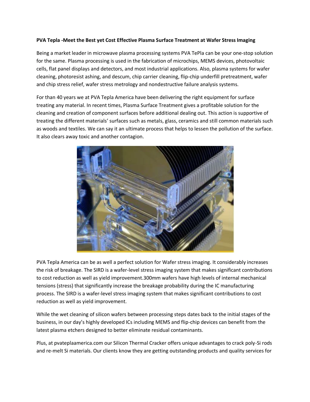
PVA Tepla -Meet the Best yet Cost Effective Plasma Surface Treatment at Wafer Stress Imaging Being a market leader in microwave plasma processing systems PVA TePla can be your one-stop solution for the same. Plasma processing is used in the fabrication of microchips, MEMS devices, photovoltaic cells, flat panel displays and detectors, and most industrial applications. Also, plasma systems for wafer cleaning, photoresist ashing, and descum, chip carrier cleaning, flip-chip underfill pretreatment, wafer and chip stress relief, wafer stress metrology and nondestructive failure analysis systems. For than 40 years we at PVA Tepla America have been delivering the right equipment for surface treating any material. In recent times, Plasma Surface Treatment gives a profitable solution for the cleaning and creation of component surfaces before additional dealing out. This action is supportive of treating the different materials’ surfaces such as metals, glass, ceramics and still common materials such as woods and textiles. We can say it an ultimate process that helps to lessen the pollution of the surface. It also clears away toxic and another contagion. PVA Tepla America can be as well a perfect solution for Wafer stress imaging. It considerably increases the risk of breakage. The SIRD is a wafer-level stress imaging system that makes significant contributions to cost reduction as well as yield improvement.300mm wafers have high levels of internal mechanical tensions (stress) that significantly increase the breakage probability during the IC manufacturing process. The SIRD is a wafer-level stress imaging system that makes significant contributions to cost reduction as well as yield improvement. While the wet cleaning of silicon wafers between processing steps dates back to the initial stages of the business, in our day’s highly developed ICs including MEMS and flip-chip devices can benefit from the latest plasma etchers designed to better eliminate residual contaminants. Plus, at pvateplaamerica.com our Silicon Thermal Cracker offers unique advantages to crack poly-Si rods and re-melt Si materials. Our clients know they are getting outstanding products and quality services for
the life span of their Plasma Etch systems. We can also assist you in the analysis of surface chemistry, contamination detection, test cleaning system effectiveness, and perform bond strength testing. Plasma Cleaning Equipment proceeds wet ability and sticking of ink, adhesives, and coatings on many different surfaces. This treatment is a reasonably priced solution for cleaning before further processing. Our plasma surface treatment equipment is used for durable adhesive bonding of plastics and metals, and we have many customizable solutions well suited your business along with your products.