Download
1 / 12
120 likes | 218 Views
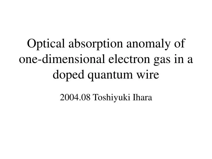
Optical absorption anomaly of one-dimensional electron gas in a doped quantum wire. 2004.08 Toshiyuki Ihara. Abstract. We measured PL and PLE spectra in an n-type doped quantum wire of superior quality, where the one-dimensional (1D) electron density (ne) is tuned by applying gate voltage.

E N D
Optical absorption anomaly of one-dimensional electron gas in a doped quantum wire 2004.08 Toshiyuki Ihara
Abstract We measured PL and PLE spectra in an n-type doped quantum wire of superior quality, where the one-dimensional (1D) electron density (ne) is tuned by applying gate voltage. At high ne, a large energy gap was observed between PL high energy cut-off and PLE onset. At low ne, we observed sharp absorption peaks which are assigned as excitons and trions. (The trion binding energy relative to the exciton peak energy is 2 meV which is larger than that reported for 2D wells.) At intermidiate ne, the peak of trion stays at the same energy with ne while the absorption peak at high ne blue-shifts rapidly from much higher energy side than the trion peak.
Introduction Memo 1 低次元電子系の光学遷移の研究について In semiconductor quantum structures which contain low-dimensional electron gas, the interband optical spectra is expected to exhibit several enhanced many-body interaction effect. - Enhancement of oscillator strength at the fermi edge appears due to the Coulomb interaction between Fermi surface electrons and a valence band hole (Fermi-edge singularity). - Binding energy of exciton , or that of trion are expected to become large with stronger quantum confinement. - Optical band-gap shrinks with an electron plasma due to the many-body Coulomb interaction (Band Gap Renormalization) - The Fermi-liquid state becomes unstable in 1D metal (Tomonaga-Luttinger Liquid) 2Dの実験と理論、1Dの現状 A lot of experimental works have been reported for n-type doped quantum wells which contain 2D electron gas and good agreements with theoretical works are reported. On the contrary, there are only few experimental reports on PL and PLE of 1D electron gas in n-type doped quantum wires. - weak emission from small aria, large disorder, difficult to control 1D electron density, difficult to achieve strong quantum confinement
Introduction Memo 2 秋山先生の論文、SSC122 (2002) 169について In this situation, we have reported PL measurement of high quality n-type doped single quantum wire, in which we tuned the electron denisty with application of an external electric field. We demontrated, in PL spectra, the large BGR of 1D plasma, 1D charged exciton with large binding energy and its evolution to Fermi-edge singularity. この論文の内容 In this paper, we report on PLE experiments in an n-type doped single quantum wire with a gate. At high ne, a large energy gap was observed between PL high energy cut-off and PLE onset. At low ne, we observed sharp absorption peaks which are assigned as excitons and trions. The trion binding energy relative to the exciton peak energy is 2 meV which is larger than that reported for 2D wells. At intermidiate ne, the peak of trion stays at the same energy with ne while the absorption peak at high ne blue-shifts rapidly from the higher energy side of the trion peak. In other words, the absorption peak at high ne does not originate from the trion peak. This is interesting because, in 2D electron gas, the trion peak is expected to evolve smoothly into the asymmetric absorption peak at high electron density. This typical optical features of 2D electron gas, which have been reported for various n-type doped quantum wells, are also observed in our experiment for 2D electron gas in one of the quantum well which composes the T-wire. By comparing the optical spectra measured on 1D and 2D electron gas in the T-wire sample, we conclude that the optical absorption anomaly on the n-type doped wire demonstrated in this report is characteristic feature of 1D electron system.
図①sample The sample was grown by the cleaved-edge overgrowth (CEO) method with molecular beam epitaxy (MBE). First, on a non-doped (001) GaAs substrate we grew a 50 nm GaAs buffer layer, a 2.26 microm barrier layer of (GaAs)9 (Al0.33Ga0.67As)71 super-lattice, a 14nm Al0.07Ga093As quantum well (stem well) layer, a 100nm Al0.33Ga0.67As spacer layer, a 4x10^11cm^-2 Si delta-doping layer, a 100nm Al0.33Ga0.67As barrier layer, a 5.66microm barrier layer of (GaAs)9 (Al0.33Ga0.67As)71 super-lattice, and a 30nm GaAs cap layer. Then, after cleaving the sample on the (110) edge, we grew, as the second MBE growth, a 6 nm GaAs quantum well (arm well) layer, a 200nm Al0.45Ga0.55As barrier layer, and a 100 nm heavily Si-doped n+ Al0.1Ga0.9As layer. As schematically shown in Fig.1, The intersection of stem well (14nm) and arm well (6nm) works as a single quantum wire. The electron density in the stem well was increased by Si delta doping. By applying DC gate voltage (Vg) to the n+ Al0.1Ga0.9As layer relative to modulation-doped 2D electron gas in the stem well, we accumulated or depleted additional electrons in the wire and the arm well. The excitation was performed via a 0.5 numerical aperture objective lens through (110) GaAs surface using cw titanium-sapphire laser. PL from the sample was collected via a (001) surface. The polarization of laser excitation and of detection are orthogonal to each other. These technique enables us to eliminate intense laser scattering and improve signal-to-noise ratio. A 0.75m single spectrometer and a liquid-nitrogen-cooled CCD camera were used to detect the PL.
図②wireの結果 Figure 2(a) shows the normalized PL (thin curve) and PLE (thick curve) spectra of the 1D wire for various gate voltages from 0 to 0.7V at 5K. The intensity of excitation light was * microW for PL measurements and * microW for PLE. At low electron density (ne), the PLE spectrum is dominated by a peak assigned as neutral exciton (X:exciton). As ne becomes higher, X peak moves away to higher energy and loses its intensity. Instead, another peak appears and becomes strong at almost 2meV below the X peak, which is assigned as trion (X-:trion), consisting of two electrons with opposite spins bound to a valence-band hole. At Vg=0.2V, the line shape of trion peak becomes asymmetric (a fast rise at low energy side and slow decay at high energy side) which is a manifest of Fermi-edge singularity. X- peak stays at the same energy with increasing ne, and above 0.2V, it becomes weak and disappears at high ne. A broad PLE onset appears at the higher energy side of X- peak and blue-shift rapidly with ne. ○: EBE △:フェルミエッジではない(フェルミエッジは◆よりも Ef×me/mhだけ下にある) ◆: EBE+Ef (1+me/mh) という可能性も捨てきれない → Ef・電子濃度・図(c)が大幅に変更される可能性も。
図②wireの結果 As we have reported in ref.*, the ne dependence of PL spectra shows the almost the same scenario. At low ne, we observed PL peak of excitons (X) and trions (X-). At high ne, the PL spectra exhibit striking lineshapes in which the onsets (band edge) of emission continuously shift to the red with increasing ne and the high-energy cutoff (Fermi edge) of emission is pinned at the position of the X- measured at small ne. Note that there is a large energy gap between the high-energy cutoff of PL and the onset of PLE. To be more quantative, we plot singular energy positions of PL and PLE spectra in Fig.2(b). Black mark corresponds to the PLE peaks. Triangles are X-, squares are X-, and diamonds are the broad peak observed at high ne. White mark corresponds to the singular energy of PL spectrum. Circles are 80% height of low energy shoulder and triangles are high energy shoulder. X peak shows blue shifts and X- shows no shift, thus, the energy gap between X and X- increases with electron density as plotted as black inverted triangles in Fig.2(c). The Fermi energy of the electrons in the wire and corresponding 1D electron density can be estimated from the energy gap between Fermi edge and Band edge in PL spectra. We plotted gate voltage dependence of the Fermi energy in Fig.2(c) and described the value of 1D electron density next to voltage value in the Fig.1(a). Figure 2(d) shows the gate voltage dependence of the intensity of PLE peaks.
図②wireの結果 Discussion Large energy gap between high energy cut-off in PL and PLE onset → ??? plasma PLE peak does not originate from X- peak. plasma PLE peak does not originate from X peak → ??? ( X peak might be stay at the same energy due to the canceling of increasing Ef and BGR) plasma PLE peak blue-shifts with almost 2×Ef → ??? energy gap between X and X- increases with electron density → increasing Ef X shows splitting → monolayer thickness fluctuations of stem well. Asymmetric line shape of trion peak → might be the power-law anomaly of FES in 1D system. Trion peak disappears at the same energy → ??? PLE intensity becomes weak rapidly at high electron density → ??? Red shift of low energy shoulder of PL → BGR ※armの結果を見せてからDiscussionにするべきかも
図③armの結果 For comparison, we conducted the same measurement on the arm well which contains 2D electron system. →測定方法 Figure 3(a) shows the normalized PL (thin curve) and PLE (thick curve) spectra of the 1D wire with various gate voltages from 0.2 to 0.8V at 5K. →励起強度 The optical features we observed here for 2D arm well are analogous to those reported by other groups. Figure 3(b) shows the singular energy positions of PL and PLE spectra of 2D arm well. →それぞれのマークの説明 In the Fig.3(c), we plotted the energy gap between X and X-, and also plotted the estimated value of Fermi energy of 2D electrons in the arm well. The electron density of 2D electron system in the arm well is described next to the gate voltage in Fig.3(a). Figure 3(d) shows the PLE peak intensity. →高濃度のPLEピークの1Dとの違い →trion binding energyの1Dとの違い →exitonの強度の電子濃度依存性の1Dとの違い
Conclusion We measured PL and PLE spectra in an n-type doped quantum wire of superior quality, where the 1D electron density (ne) is tuned by applying gate voltage. At high ne, a large energy gap was observed between PL high energy cut-off and PLE onset. At low ne, we observed sharp absorption peaks which are assigned as excitons and trions. (The trion binding energy relative to the exciton peak energy is 2 meV which is larger than that reported for 2D wells.) At intermidiate ne, the peak of trion stays at the same energy with ne while the absorption peak at high ne blue-shifts rapidly from much higher energy side than the trion peak. In other words, the absorption peak at high ne does not originate from the trion peak in 1D electron system. By comparing the optical spectra measured on 1D and 2D electron gas in the T-wire sample, we conclude that the optical absorption anomaly on the n-type doped wire demonstrated in this report is characteristic feature of 1D electron system.
Reference例① 1Akiyama et. al. , Solid State Communications 122 (2002) 169 1D doped T-Wire / density dependence of PL / X,X-,plasma emission / PL weak FES 2Takagiwa et. al. , JPCS 63 (2002) 1587 Theory : 2DEG / density dependence of FES in absorption spectra / X,X-,Continuum 3Laruelle, PRB, 65 (2002) 195303 1D doped LSL / PL at high density / strong FES by Fano resonance 4Laruelle, PRB, 65 (2002) 195302 1D doped LSL / PL and PLE at high density / Moss-Burstein shift / no 1D features 5Kapon, Physica E, 11 (2001) 224 1D doped V-groove / PL, PLE at high density / PL FES (?) / PLE weak FES (?) 6Kaur, phys. Stat. sol. A 178,465 (2000) 2D doped 10nm well / density dependence of PL, PLE / X,X-,continuum / FES 7Yusa, PRB 62 15390 (2000) 2D doped 20nm well / density dependence of PL,photocurrent / X,X- / FES of X 8V. Huard, PRL 84 (1999) 187 2D CdTe doped 10nm well / density dependence of absorption / X,X- / w2-w1=EF+Eb 9Kim, Physica E7 517 (2000) 1D doped v-groove / PL / FES at n=2 10Brown, PRB 54 (1996) R11082 2D doped 5nm well / density dependence of absorption / X,X- but hard to resolve 11Finkelstein, PRL 74 (1995) 976 2D doped 20nm well / density dependence of PL,PLE / X,X-,plasma 12Sekiyama, PRB 51 (1995) 13899 Cu salt / PL / Fermi-liquid or Luttinver-liquid 13G.D Mahan, Phys. Rev. 153 (1967) 882 Theory : 3D Metal / x-ray absorption / power-law divergent in absorption spectra 14Hawrylak, Phys. Rev. B44 (1991) 3821 Theory : 2D electron system / emission, absorption / X, X- / power-law divergent 15Nozieres et al. Phys. Rev. 178 (1969) 1097 Theory : 3D metal / x-ray absorption / reduced FES by Anderson infrared catastrophe 16Combescot, J. Phys. (Paris) 32 (1971) 1097 Theory : 2D electron system / absorption of X, continuum / power-law divergent