Download
1 / 30
300 likes | 309 Views
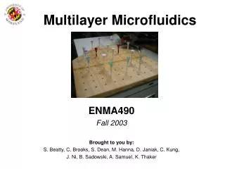
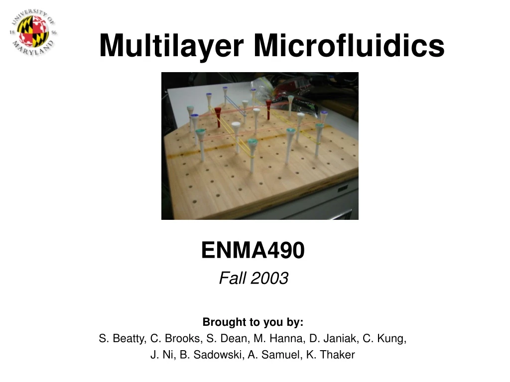
Multilayer Microfluidics. ENMA490 Fall 2003 Brought to you by: S. Beatty, C. Brooks, S. Dean, M. Hanna, D. Janiak, C. Kung, J. Ni, B. Sadowski, A. Samuel, K. Thaker. Problem Definition. Motivation BioMEMS research is growing rapidly, but restricted to single layer microfluidics

E N D
Multilayer Microfluidics ENMA490 Fall 2003 Brought to you by: S. Beatty, C. Brooks, S. Dean, M. Hanna, D. Janiak, C. Kung, J. Ni, B. Sadowski, A. Samuel, K. Thaker
Problem Definition Motivation • BioMEMS research is growing rapidly, but restricted to single layer microfluidics • Development of a multilayer microfluidic design would increase flexibility Goal • Design, construct, and test a controllable microfluidic device with at least two fluid levels • Identify appropriate materials, processes, and device geometries
Problem Scope Requirements • To make a two-level microfluidic device • To incorporate active control elements Constraints • Assume external fluid control • Neglect biochemical reactions in channels • Keep design feasible for manufacturing
Initial Material Choices Desired Characteristics • Ease of patterning and use in microfabrication • Chemically inert • Low Cost / Obtainable • Optically transparent • Specific Elastic modulus (flexible, rigid)
Initial Material Choices Substrate Material • Silicon • Relatively inexpensive • Commonly used in microelectronics • Well known properties and processing techniques • Pyrex • Transparent to visible light • Allows visual monitoring of micro channels • More expensive than silicon
Initial Material Choices Microchannel Material • Poly(dimethylsiloxane) or PDMS • Inexpensive • Poor surface adhesion – releasable from mold • Highly flexible • modulus of 2.5 MPa • SU-8 • Is a photoresist • High aspect ratios obtainable • Good surface adhesion to silicon and pyrex • Very rigid – complementary to PDMS • modulus of 4000 MPa
Defined Problem Divided into research groups (BioMEMS, Materials, Devices, and Circuits) Modified design to integrate vertical vias for multilevel fluid flow Developed Stage 1 (Initial Microchannel Design Concept) Developed fluid control device to manipulate fluid flow Developed and tested Stage 2 (Modified Microchannel Design) Developed and tested Stage 3 (Final Design: Pressure Actuated Valve Design) Summarized manufacturing and experimental results of final design ProjectDevelopment
Device Design: Stage 1(Initial Microchannel Design Concept) • Objective • To create an initial design for a multilayer micro fluidic device • Initial design elements • 90o orientation of fluid layers • Vertical interconnects at channel intersections • Each layer has same design- reduces number of molds • Versatility of fluid paths I/O Bottom layer I/O Middle layer Top layer
Device Design: Stage 1 (Initial Microchannel Design Concept) • Materials • Stackable PDMS layers • Silicon substrate • SU-8 molds • Processes • Create a channel mold and an interconnect mold using SU-8 • Create PDMS layers from SU-8 mold: two layers from channel mold, one interconnect layer • Stack layers on substrate starting with a channel layer, interconnect layer and second channel layer at 90o orientation
Device Design: Stage 2(Modified Microchannel Design) Objective • To test the viability of a two-level passive micro-fluidic device Modifications from Stage 1 • Moved reservoir positions to fit existing packaging • Created discrete flow paths to test flow on individual layers and between layers • Increased all dimensions to facilitate fabrication and testing Device Logic • Five distinct fluid paths • 11 I/O • Two distinct channel levels • One interconnect level • One Top Cover level
Device Design: Stage 2(Modified Microchannel Design) Device Geometry • Chosen for process compatibility • Rectangular micro-channels • Square Interconnects • Circular reservoirs Materials • SU-8 used as a mold for the PDMS layers • All PDMS layers stacked on a Silicon substrate
Micro-Channel Layer 1 Interconnect Layer Micro-Channel Layer 2 Top Cover Layer Device Design: Stage 2(Modified Microchannel Design) Process Sequence and Mask Design • Begin with four polished Si wafers • Spin SU-8 (negative photoresist) on the Si wafers and pre-bake at 95°C • Align each of the four wafers with one of the four masks shown below and expose the SU-8 to ultraviolet light, then post-bake at 95°C • Develop the SU8 so that the unexposed areas are removed • Results in four distinct SU8 molds
Micro-Channel Layer 1 Interconnect Layer Micro-Channel Layer 2 Top Cover Layer Device Design: Stage 2(Modified Microchannel Design) 5. Spin PDMS on the SU8 molds less than the vertical dimension of the SU-8 protrusions • Mix PDMS (Sylgard 184, Dow-Corning) 10:1 with curing agent • Spin on PDMS • Dip the Si wafer in a sodium dodecyl sulfate(SDS) adhesion barrier and allow it to dry naturally • Bake in box furnace for 2 hours at 70°C 6. Delaminate and stack all four PDMS layers in the following order: Micro-channel Layer 1, Interconnect Layer, Micro-channel layer 2, Top Cover Layer
Device Design: Stage 2(Modified Microchannel Design) Final Expected Result:
Stage 2: Experimental Trial 1 • Top layer interconnects did not go through, so we had to poke holes with the needle • Caused problems with sealing around the needle and getting pressure to move liquid through the channels and not out at the opening • Interconnects did not connect, so liquid would not flow at all in any of those channels • Many layers were delaminated or had giant air bubbles, which liquid would spread out into
Stage 2 Experimental Trial • Fabrication • Successfully made and aligned four layers • Layers had very few defects • All interconnects joined two different layers • Entire wafer looked very good- no rough edges, no air bubbles between layers, no craters
Successfully got liquid to flow in all channels using pressure from a syringe Were able to push liquid all the way through 2 out of five channels Used three different colors of food coloring, so we can see the areas where the fluid reached Needle opening was too large, and angle of needle opening made use difficult Had to force the needle into the channels to obtain any pressure, and this sometimes delaminated the layers around the channel Solved this by inserting the needle opening into the channel and sealing the opening with a finger on top of the needle Stage 2 ExperimentalSuccesses & Problems
2nd Experimental Problems Continued • No capillary action effects were observed (all liquid movement was obtained with pressure) • In many cases, the pressure required to push the liquid through the channels exceeded the adhesion forces between the layers, so layers came apart and liquid stopped flowing through the channel • This was also solved with applied force from a few fingers in some cases • Could have also been too much pressure applied with syringe
Device Design: Stage 3(Pressure Actuated Valve Test Design) Device Objective • To integrate an active control element into a basic microchannel design based on Stage 2 Modifications from Stage 2 • Removed all microchannels except for T-shaped section • Added a completely top layer microchannel • Incorporated negative pressure gas valves in design (Figure _) Device Logic • Two distinct fluid paths • Five I/O • Two channel levels • One gas channel level • One thin flex layer • One top cover layer
Device Design: Stage 3(Pressure Actuated Valve Test Design) Device Objective • To integrate an active control element into a basic microchannel design based on Stage 2 Modifications from Stage 2 • Removed all microchannels except for T-shaped section • Added a completely top layer microchannel • Incorporated negative pressure gas valves in design (Figure _) Device Logic • Two distinct fluid paths • Five I/O • Two channel levels • One gas channel level • One thin flex layer • One top cover layer
Device Design: Stage 3(Pressure Actuated Valve Test Design) Device Geometry • Made for feasibility • 4 gas control sites • 1 fluid interconnect • Thin PDMS flex layer Materials • SU-8 for rigid portions in valve design (gate) • SU-8 for fluid layers • PDMS for gas control layer • PDMS used for flexible gas/fluid membrane • 2 substrates required (Si, Pyrex)
Rr + Rc + Ri + Rv RTotal Device Design: Stage 3(Pressure Actuated Valve Design) Fluid Flow Modeling • Assumed Fluid Flow Rate based on Fluid velocity • Based on literature search: 1500 cm/minute= 2.5 E5 μm/sec • 1.25 E 10 μm3/sec= 0.0125 cm3/sec • Fluidic Resistance: R= ΔP/Q [(N*s)/m5] • R(circular cross section)= 8μL/(πr4) • μ= Fluid Viscosity= 0.01 g/sec*cm • L= Length of channel • r= Radius of channel • R(Rectangular cross section)~ 12μL/(wh3) • w= Width of the channel • h= Height of the Channel • Total Fluidic Resistance = Rr + Rc + Ri + Rv
Device Design: Stage 3(Pressure Actuated Valve Design) Fluid Flow Modeling • Determined the velocity, fluidic resistance, Reynolds number, and pressure gradient in each section of the fluids path and found the relevant total fluid path properties Sample output for the two valve fluid path • Total Pressure Gradient • ~15330Pa~115 Torr • Pressure Gradient at the Valve • 3750 Pa~28 Torr • Fluid Flow Rate • 1.25 E 10 μm3/sec= 0.0125 cm3/sec • Total Cycle Time • ~21.2 seconds
Processing Problems • Substantial amount of cracks in SU-8 layer • Layer alignment problems • Razor blade/ tweezers method • Layer thickness • Wrinkles • Air pockets Cracks in reservoir region of SU-8 mold
Processing Problems Continued • Feature alignment • Extremely difficult • Inaccurate • Interconnect layer • No connection provided • Problem with layer thickness
Alternative Designs • Phase Change Bubble Valve • Design Elements • Isolated fluid chamber • Membrane division between chamber and fluid channel • Stopper to aid in the control of the fluid • Principles of Actuation • Volatile liquid (cyclopentane) • Resistive heaters • Heater cause fluid to change from liquid to gas • Expansion form gas pressure deflects membrane
Alternative Designs • Phase Change Bubble Valve • Associated Problems • How much pressure is needed to deflect membrane • How much power is needed to create enough heat • How quick is the reverse reaction
Alternative Designs (Piezoelectric) • Piezoelectric Valve • Design Elements • Isolated liquid chamber • Membrane division between chamber and fluid channel • Partial gate to aid in closing of valve • Principles of Actuation • Piezoelectric material electrically activated • Expansion causes compression in liquid chamber • Compression translated to membrane deformation with larger amplitude
Future Work Here are a few material changes we would pursue if time allowed: • Replace Pyrex with acrylic for the top substrate • Promote adhesion or a seal between the PDMS layers • Alter surface chemistry of the channels to be hydrophilic