Download
1 / 25
610 likes | 1.87k Views
Electron diffraction. Selected area diffraction (SAD) in TEM Electron back scatter diffraction (EBSD) in SEM. Bragg’s law.

E N D
Electron diffraction Selected area diffraction (SAD) in TEM Electron back scatter diffraction (EBSD) in SEM MENA3100
Bragg’s law Bragg’s law tells you at which angle θB to expect maximum diffracted intensity for a particular family of crystal planes. For large crystals, all other angles give zero intensity. The Ewald Sphere Cu Kalpha X-ray: = 150 pm Electrons at 200 kV: = 2.5 pm k ko g The observed diffraction pattern is the part of the reciprocal lattice that is intersected by the Ewald sphere MENA3100
2θ k ko First order Laue zone Zero order Laue zone g Intensity distribution and Laue zones Ewald sphere (Reflecting sphere) The intensity distribution around each reciprocal lattice point is spread out in the form of spikes directed normal to the specimen MENA3100
Multiple scattering (diffraction) leads to oscillations in the diffracted intensity with increasing thickness of the sample Forbidden reflection may be observed Kinematical intensities with XRD Incident beam Multiple scattering Multiple diffracted beam Transmitted beam Diffracted beam MENA3100
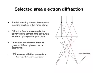
3,8 Å 1,1 nm Simplified ray diagram Parallel incoming electron beam Si Sample Objective lense Diffraction plane (back focal plane) Objective aperture Selected area aperture Image plane MENA3100
Apertures Condenser aperture Objective aperture Selected area aperture MENA3100
Poly crystalline sample Four epitaxial phases Diffraction with large SAD aperture, ring and spot patterns Similar to XRD from polycrystalline samples. The orientation relationship between the phases can be determined with ED. MENA3100
Film plate Camera constant R=L tan2θB ~ 2LsinθB 2dsinθB =λ ↓ R=Lλ/d Camera constant: K=λL MENA3100
(h2k2l2) Indexing diffraction patterns The g vector to a reflection is normal to the corresponding (h k l) plane and IgI=1/dnh nk nl • Measure Ri and the angles between • the reflections • - Calculate di , i=1,2,3 (=K/Ri) • Compare with tabulated/theoretical • calculated d-values of possible phases • Compare Ri/Rj with tabulated values for • cubic structure. • g1,hkl+ g2,hkl=g3,hkl (vector sum must be ok) • Perpendicular vectors: gi● gj = 0 • Zone axis:gi x gj=[HKL]z • All indexed g must satisfy: g ● [HKL]z=0 Orientations of corresponding planes in the real space MENA3100
BiFeO3 Pt TiO2 Lim SiO2 Si 200 nm Example: Study of unknown phase in a BiFeO3 thin film Metal organic compound on Pt Heat treatment at 350oC (10 min) to remove organic parts. Process repeated three times before final heat treatment at 500-700 oC (20 min) . (intermetallic phase grown) Goal: BiFeO3 with space grupe: R3C and celle dimentions: a= 5.588 Å c=13.867 Å MENA3100
27o 50 nm 15o 10o 0o Determination of the Bravais-lattice of an unknown crystalline phase Tilting series around common axis MENA3100
0o 50 nm 19o 25o 40o 52o Determination of the Bravais-lattice of an unknown crystalline phase Tilting series around a dens row of reflections in the reciprocal space Positions of the reflections in the reciprocal space MENA3100
011 111 001 101 6.04 Å 8.66 Å [101] [011] 7.94 Å 010 110 100 c b a Bravais-lattice and cell parameters [100] d = L λ / R From the tilt series we find that the unknown phase has a primitive orthorhombic Bravias-lattice with cell parameters: a= 6,04 Å, b= 7.94 Å og c=8.66 Å α= β= γ= 90o MENA3100
O - K Fe - L2,3 BiFeO3 Ukjent fase 500 eV forskyvning, 1 eV pr. kanal Chemical analysis by use of EDS and EELS Ukjent fase BiFeO3 BiFe2O5 MENA3100
Published structure A.G. Tutov og V.N. Markin The x-ray structural analysis of the antiferromagnetic Bi2Fe4O9 and the isotypical combinations Bi2Ga4O9 and Bi2Al4O9 Izvestiya Akademii Nauk SSSR, Neorganicheskie Materialy (1970), 6, 2014-2017. Romgruppe: Pbam nr. 55, celleparametre: 7,94 Å, 8,44 Å, 6.01Å x y z Bi 4g 0,176 0,175 0 Fe 4h 0,349 0,333 0,5 Fe 4f 0 0,5 0,244 O 4g 0,14 0,435 0 O 8i 0,385 0,207 0,242 O 4h 0,133 0,427 0,5 O 2b 0 0 0,5 Celle parameters found with electron diffraction (a= 6,04 Å, b= 7.94 Å and c=8.66 Å) fits reasonably well with the previously published data for the Bi2Fe4O9 phase. The disagreement in the c-axis may be due to the fact that we have been studying a thin film grown on a crystalline substrate and is not a bulk sample. The conditions for reflections from the space group Pbam is in agreement with observations done with electron diffraction. Conclusion: The unknown phase has been identified as Bi2Fe4O9 with space group Pbam with cell parameters a= 6,04 Å, b= 7.94 Å and c=8.66 Å. MENA3100
θB θB 2θB Objective lens Diffraction plane Excess line Deficient line 1/d Kikuchi pattern • Inelastically scattered electrons • give rise to diffuse background in the ED pattern. • Angular distribution of inelastic scattered electrons falls of rapidly with angle. I=Iocos2α • Kikuchi lines are due to: • Inelastic+ elastic scattering event Excess Deficient • Used for determination of: • crystal orientation • -lattice parameter • -accelerating voltage • -Burgers vector http://www.doitpoms.ac.uk/index.html http://www.doitpoms.ac.uk/tlplib/diffraction-patterns/kikuchi.php MENA3100
Electron Back Scattered Diffraction (EBSD)Orientation Image Microscopy (OIM) in a SEM • EBSD • Geometry similar to Kikuchi diffraction in TEM • Information from nm regions • OIM • Gives the distribution of crystal orientation for grains intersected by the sample section that can be presented in various ways. (+/- 0.5o) • Involves • collection a large sets of EBSD data • Bin the crystallographic data from each pixel (stereographic triangle) • Colour codes • Localized preferred orientation and residual stress etc. MENA3100
Orientation map example CD-200 Nordiff EBSD Camera Step=0.2micron MENA3100
Overlaid maps MENA3100
Electron back scattered diffraction (EBSD) Principal system components Sample tilted at 70° from the horizontal, a phosphor screen, a sensitive CCD video camera, a vacuum interface for mounting the phosphor and camera in an SEM port. Electronic hardware that controls the SEM, including the beam position, stage, focus, and magnification. A computer to control EBSD experiments, analyse the EBSD pattern and process and display the results. http://www.ebsd.com/ebsd-explained/anim2.htm http://www.ebsd.com/ebsd-explained/simulationapplet.htm MENA3100
Microscope operating conditions Probe current Increased probe current – shorter camera integration time – increased beam size Accelerating voltage Increased accelerating voltage – reduced λ - reduced width of the Kikuchi bands – brighter pattern - shorter integration time – higher penetration depth Changing the accelerating voltage may require adjustment to the Hough transform filter size to ensure the Kikuchi bands are detected correctly 20 kV 30 kV 10 kV Effect of changing accelerating voltage on diffraction patterns from nickel MENA3100
Microscope operating conditions Working distance and magnification Because the sample is tilted, the SEM working distance will change as the beam position moves up or down the sample, and the image will go out of focus. Image without tilt or dynamic focus compensation Image with tilt compensation and no dynamic focus compensation Image with tilt and dynamic focus compensation. The working distance is 14.98 mm at the top and 15.11 mm at the bottom of the image MENA3100
Microscope operating conditions EBSD systems can compensate automatically for shifts in the pattern centre by calibrating at two working distances and interpolating for intermediate working distance values. It is important to know the range of working distances for which the EBSD system will remain accurately calibrated. With a tilted sample, the pattern centre position will depend on the sample working distance. The yellow cross shows the pattern centre with working distance 10, 18 and 22 mm MENA3100
Band Intensity The mechanisms giving rise to the Kikuchi band intensities and profile shapes are complex. As an approximation, the intensity of a Kikuchi band for the plane (hkl) is given by: where fi(θ) is the atomic scattering factor for electrons and (xi yi zi) are the fractional coordinates in the unit cell for atom i. An observed diffraction pattern should be compared with a simulation to ensure only planes that produce visible Kikuchi bands are used when solving the diffraction pattern. Simulated diffraction pattern showing all Kikuchi bands with intensity greater than 10% of the most intense band. Simulation of crystal orientation giving the solution shown. Diffraction pattern from the orthorhombic ceramic mullite (3Al2O3 2SiO2) collected at 10 kV accelerating voltage. Solution overlaid on the diffraction pattern giving the crystal orientation as {370}<7-34> MENA3100
Background removal The background can be measured by scanning the beam over many grains in the sample to average out the diffraction information. The background can be removed by subtraction from, or division into, the original pattern. Original pattern Background subtraction Background division Background http://www.ebsd.com/ebsd-explained/undertakingexperiments3.htm MENA3100