Download
1 / 1
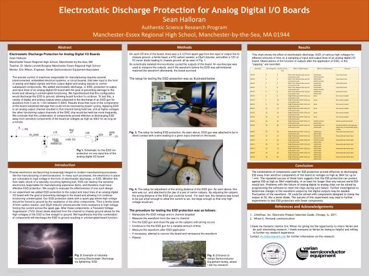
20 likes | 167 Views
Electrostatic Discharge Protection for Analog Digital I/O Boards. Methods. Abstract.

E N D
Electrostatic Discharge Protection for Analog Digital I/O Boards Methods Abstract Precise electronics are becoming increasingly integral to modern manufacturing processes, like the manufacturing of semiconductors. In many such processes, the electronics in place are vulnerable to high voltage in the form of electrostatic discharge, or ESD. Whether this from static shock or a naturally-occurring lightning bolt, ESD can destroy the sensitive electronics responsible for manufacturing expensive items, and therefore must have effective ESD protection. We sought to evaluate the effectiveness of one such design. In our experiment we added ESD protection to the output and input lines of an analog digital I/O board with the goal of preventing damage to the board and allowing it to continue functioning uninterrupted. Our ESD protection starts with a spark gap where high voltage should be forced to ground by the resistance of the other components. Then a ferrite bead, 47ohm carbon resistor, and 33µH inductor should provide more resistance to high voltage forcing the current across the spark gap. After these components, a Transient Voltage Suppression (TVS) Zener diode attached from the channel to chassis ground allows for the high voltages of the ESD to flow straight to ground. We hypothesize that this combination of components will discharge the ESD to ground resulting in uninterrupted board function. Introduction This chart shows the effect of electrostatic discharge, ESD, of various high voltages for different amounts of time on a sampling of input and output lines of an analog digital I/O board. Observations of the function of outputs after the application of ESD, or the “zapping,” are recorded. Results On each I/O line of the board, there was a 0.127mm spark gap from the input or output line to chassis ground, a ferrite bead, a 47Ω carbon resistor, a 33µH inductor, and either a 12V or 5V zener diode leading to chassis ground, all as seen in Fig. 1. An eclectically isolated microcontroller cycled the outputs of the board. An oscilloscope was used to measure the outputs, and if the waveform before the ESD was administered matched the waveform afterwards, the board survived. The setup for testing the ESD protection was as illustrated below. Fig. 3. The setup for testing ESD protection. As seen above, ESD gun was attached to be in direct contact with a wire leading to a given input channel on the board. Fig. 4. The setup for adjustment of the arcing distance of the ESD gun. As seen above, this wire was cut and attached to the jaw of a pair of venire calipers. By adjusting the calipers, the arcing distance of the ESD gun could be tuned. For each test, this distance was tuned to be just small enough to allow the current to arc, but large enough so that only high voltage would arc. The procedure for testing the ESD protection was as follows: Manipulate the ESD voltage and i/o channel targeted Measure the waveform from the new i/o channel Fire the ESD gun and close the gap on the calipers until arcing occurs Continue to fire the ESD gun for a variable amount of time Measure the waveform after ESD application If necessary, attempt to recover the board and remeasure the waveform Repeat The combination of components used for ESD protection proved effective at discharging ESD away from sensitive components of the board at voltages as high as 30kV for up to 1 min. The repeated success of these tests suggests that the ESD protection can protect against ESD as high as 30kV indefinably, or at least for longer than any natural world ESD would last. Problems with the failure of analog digital to analog chips can be solved by programming the software to reset the chips during such failure. Further investigation to determine changes in the waveform output by the digital outputs may be needed. Fluctuation of the waveform ~5V could be solved with components designed to clamp the output at 5V, like a zener diode. The success of this experiment may lead to further experiments to test ESD protection with fewer components. References and Acknowledgements 1. Littelfuse, Inc. Electronic Product Selection Guide, Chicago, IL, 2011. Wilson E. Personal communication I thank my fantastic mentor Eric Wilson for giving me the opportunity to intern Varian and do such interesting research. I thank everyone at Varian for being so helpful and willing to further my research experience. Contact sh.redsox@gmail.com for further information on this research. Authentic Science Research Program Manchester-Essex Regional High School, Manchester-by-the-Sea, MA 01944 Sean Halloran Electrostatic Discharge Protection for Analog Digital I/O Boards Sean Halloran Manchester Essex Regional High School, Manchester-by-the-Sea, MA Teacher, Dr. Maria Lonnett Burgess Manchester Essex Regional High School Mentor, Eric Wilson, Engineer, Varian Semiconductor Equipment Associates The precise control of machines responsible for manufacturing requires several interconnected, embedded electrical systems, or circuit boards, that take input in the form of analog and digital signals and then output digital and analog signals to control subsequent components. We added electrostatic discharge, or ESD, protection to output and input lines of an analog digital I/O board with the goal of preventing damage to the board and allowing it uninterrupted functioning. We hypothesized that this configuration would discharge the ESD to ground, allowing board function to continue. To test this, a variety of digital and analog outputs were subjected to the discharge of an ESD gun for durations from 3 sec to 1 min between 5-20kV. Results show that none of the components of the board sustained damage that could not be resolved by power cycling. Applying ESD to an analog output channel resulted in that channel being held low, and at higher voltages the other functioning output channels of the DAC chip would be held low more frequently. We conclude that this combination of components proved effective at discharging ESD away from sensitive components of the board at voltages as high as 30kV for as long as a minute. Conclusion Fig 1. Schematic for the ESD ion protection on one input line of the analog digital I/O board Fig. 2. Example of naturally-occurring Electrostatic Discharge via lightening, ESD Fig. 5. Entrance to Varian Semiconductor Equipment facility, where I did my research.