Download
1 / 12
120 likes | 199 Views
Finding Best Voltage and Frequency to Shorten Power Constrained Test Time. Praveen Venkataramani Suraj Sindia Vishwani D. Agrawal. Introduction. ATPG generated scan patterns produce more circuit activity than the functional patterns.

E N D
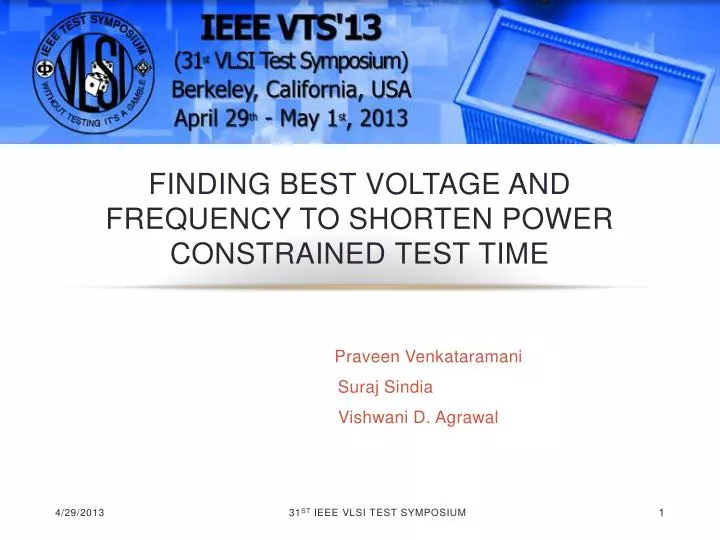
Finding Best Voltage and Frequency to Shorten Power Constrained Test Time Praveen Venkataramani Suraj Sindia Vishwani D. Agrawal 31st IEEE VLSI Test Symposium
Introduction • ATPG generated scan patterns produce more circuit activity thanthe functional patterns. • Scan test cause high power dissipation during scan shift and capture. • Power Constrained Test: • Limit the maximum power dissipation to stay within rated power for the device • Slow down the clock • Modify test vectors to reduce activity • Result: A general increase in test time 31st IEEE VLSI Test Symposium
Reducing Supply Voltage • Power reduces. • If power constrained, test clock may be speeded up to reduce test time. • Critical path delay increases. • Certain defects are more profound at low voltages. • Changes in critical paths possible. 31st IEEE VLSI Test Symposium
Definitions • Power constraint • Maximum power dissipated by test is limited by the maximum allowable power. • Maximum activity test cycle determines the test clock frequency. • Structure constraint • Clock frequency is determined by the critical path delay. • Fastest test/functional clock period cannot be smaller than the critical path delay • Test at lower voltage tends to become structure constrained. • Slowing the clock to reduce power increases test time. • Speeding up the clock increase power. 31st IEEE VLSI Test Symposium
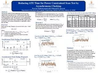
Power and Structure Constrained Testing 11 Structure-constrained operation Power-constrained operation Power-constrained clock Peak per vector power of test Clock frequency Power +Δf PMAXfunc Structure-constrained clock Test clock – ΔVDD Nom. VDD Opt. VDD Voltage, VDD From an ITC’12 Elevator Talk Reduced Voltage Test Can be Faster! by Vishwani Agrawal 31st IEEE VLSI Test Symposium
Analysis of Power Constrained Test • The minimum test clock period for a set of ATPG test clock cycles is limited by the maximum allowable power • Quantitatively: where EMAXtestis the maximum energy dissipated during a test cycle PMAXfuncis the maximum allowable power • TPOWER is a function of voltage • Now, the total test time is then given by* where , is the number of clock cycles. * M. L. Bushnell and V. D. Agrawal, Essentials of Electronic Testing for Digital, Memory and Mixed-Signal VLSI Circuits, Springer, 2000, Chapter 14. 31st IEEE VLSI Test Symposium
Analysis of Structure Constrained Test • Critical path delay of a circuit can be approximated using α-power law model* where VDDis the supply voltage VTH is the threshold voltage K is a proportionality constant αis velocity saturation index • Decrease in VDD increases delay • Total test time is given by * T. Sakurai and A. R. Newton, “ASimple MOSFET Modelfor Circuit Analysis,” IEEE Journal of Solid-State Circuits, Vol. 26, pp.122–131, Feb. 1991. 31st IEEE VLSI Test Symposium
Assumptions • Critical path does not change as voltage is reduced; found valid for small voltage changes. • Threshold voltage remains constant. 31st IEEE VLSI Test Symposium
Optimum Test Time • For any supply voltage, test clock frequency or test clock period • Test time for power constrained test can be reduced by reducing the supply voltage • Critical path delay increases with reduction in supply voltage • Optimum test time for power constrained test is the point at which the test clock runs fastest while the operation is still power constrained; • Optimum voltage can be obtained by solving for voltage 31st IEEE VLSI Test Symposium
Example - s298 31st IEEE VLSI Test Symposium
Optimum Test Time Results 31st IEEE VLSI Test Symposium
Conclusion • What we have achieved • Optimum test time for power constrained test • Optimum voltage and frequency for power constrained tests • Future explorations • Consideration of separate critical paths for scan and functional logic • Delay testing at reduced voltage • Adaptive dynamic power supply • Dynamic test frequency 31st IEEE VLSI Test Symposium