Download
1 / 12
120 likes | 128 Views
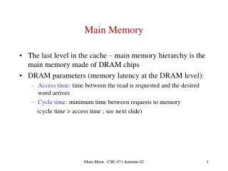
Main memory. Recall that on a cache miss, need to access memory. Takes 3 steps (e.g., for a read) Send the address Get the contents of the memory locations (at the DRAM level) Transfer the contents to the cache DRAM parameters (memory latency at the DRAM level):

E N D
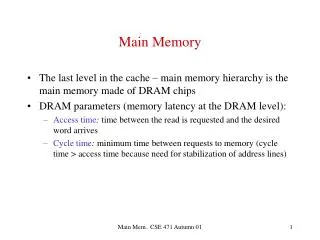
Main memory • Recall that on a cache miss, need to access memory. Takes 3 steps (e.g., for a read) • Send the address • Get the contents of the memory locations (at the DRAM level) • Transfer the contents to the cache • DRAM parameters (memory latency at the DRAM level): • Access time: time between the read is requested and the desired word arrives • Cycle time: minimum time between requests to memory (cycle time > access time because need for stabilization of address lines) CSE 471 Main Memory
DRAM’s • Address lines split into row and column addresses. A read operation consists of: • RAS (Row access strobe) • CAS (Column access strobe) • If device has been precharged, access time = RAS + CAS • If not, have to add precharge time • RAS, CAS, and Precharge are of the same order of magnitude • In DRAM data needs to be written back after a read, hence cycle time > access time CSE 471 Main Memory
DRAM array Row address page Page buffer Column address CSE 471 Main Memory
DRAM and SRAM • D stands for “dynamic” • Each bit is single transistor (plus capacitor; hence the need to rewrite info after a read) • Needs to be recharged periodically. Hence refreshing. All bits in a row can be refreshed concurrently (just read the row). • For each row it takes RAS time. • S stands for “static” • Uses 6 transistors/bit (some use 4). No refresh and no need to write after read (i.e., information is not lost by reading). CSE 471 Main Memory
DRAM vs. SRAM • Cycle time of SRAM 10 to 20 times faster than DRAM • For same technology, capacity of DRAM 5 to 10 times that of SRAM • Hence • Main memory is DRAM • On-chip caches are SRAM • Off-chip caches (it depends) • DRAM growth • Capacity: Factor of 4 every 3 years (60% per year) • Cycle time. Improvement of 20% per generation (7% per year) CSE 471 Main Memory
How to improve main memory bandwidth • It’s easier to improve on bandwidth than on latency • Sending address: can’t be improved (and this is latency) • Although split-transaction bus allows some overlap • Make memory wider (assume monolithic memory) • Sending one address, yields transfer of more than one word if the bus width allows it (e.g., Alpha 21064 has L2, DRAM, and memory bus all 256 bits wide) or even if it does not allow it (see interleaving next slide) • But less modularity (buy bigger increments of memory) • Requires ECC on a word basis (or on the basis of the minimum write information unit). Otherwise need of “read-modify-write” when writes occur. CSE 471 Main Memory
Interleaving (introducing parallelism at the DRAM level) • Memory is organized in banks • Bank i stores all words at address j modulo i • All banks can read a word in parallel; Number of banks should match the L2 block size • Bus does not need to be wider (buffer in the DRAM bank) • Writes to individual banks for different addresses can proceed without waiting for the preceding write to finish (great for write-through caches) • Banks of banks • interleaving on low order bits for sequential access (all words in a block) and other bits for parallel access (for lock-up free caches and for multiprocessors sharing main memory) CSE 471 Main Memory
Limitations of interleaving • Number of banks limited by increasing chip capacity • With 1M x 1 bit chips, it takes 64 x 8 = 512 chips to get 64 MB (easy to put 16 banks of 32 chips) • With 16 M x 1 chips, it takes only 32 chips (only one bank) • More parallelism in using 4M x 4 chips (32 chips in 4 banks) CSE 471 Main Memory
Memory path of workstation DRAM L2 Bank 0 Memory bus Data switch CPU + L1 16B 32B Processor bus Bank n To/from I/O bus CSE 471 Main Memory
Page-mode and Synchronous DRAMs • Introduce a page buffer • In page mode no need for a RAS • But if a miss, need to precharge + RAS + CAS • In SDRAM, same as page-mode but subsequent accesses even faster (burst mode) CSE 471 Main Memory
Rambus • Specialized memory controller (scheduler), channel, and DRAM’s • Parallelism and pipelining, e.g. • independent row , column, and data buses (narrow -- 2 bytes) • pipelined memory subsystem (several packets/access) • parallelism within the DRAMs (many banks with 4 possible concurrent operations) • parallelism among DRAM’s (large number of them) • Great for “streams of data” (Graphics, games) CSE 471 Main Memory
Split-transaction bus • Allows transactions (address, control, data) for different requests to occur simultaneously • Required for efficient Rambus • Great for SMP’s sharing a single bus CSE 471 Main Memory