Download
1 / 16
160 likes | 256 Views
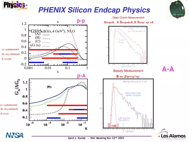
GS95. PHENIX Silicon Endcap Physics. Open Charm Measurement D=> m +X, D D=> m +e+X, D D=> m + + m - +X. p-p. cc (displaced)X. bb e/ +displaced. B J/ Xg. A-A. Beauty Measurement B => J/ y=>m + +m -. p-A. cc (displaced)X. bb e/ +displaced. B J/ X. /100.

E N D
GS95 PHENIX Silicon Endcap Physics Open Charm Measurement D=>m+X, DD=>m+e+X, DD=>m+ +m- +X p-p cc(displaced)X bbe/+displaced BJ/Xg A-A Beauty Measurement B => J/y=>m++m- p-A cc(displaced)X bbe/+displaced BJ/X /100
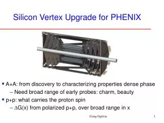
PHENIX Silicon Endcap • Executive Summary • Four umbrella stations on each side matching the large MUON arm acceptace • Mini-strips of 50mu * 2.2 -13 mm (not the BNL detector for S/N reasons) • Readout via new PHX chip from Fermilab (based on existing FNAL chip architecture) • Data push via ~3 Gigabit optical links • Total channel count: 2 Million channels • Total chip count: 4000 chips B -> J/y->m++m-
4608 4096 Preliminary 11/03 Si Umbrella Layout • 50 mu radial pitch (z vertex reconstruction) • 4608 (4096) “mini-strips” • 3.5 cm < r < 18 (14) cm • < 1 % occupancy • 48 “double towers” in phi • mini-strips from 13.0 mm to 2.2 mm • 2 rows of strips per “double tower”, readout via one chip row r = 18.0 cm r = 14.0 cm r = 3.5 cm 1
Collaboration with FNAL • Started to work with Ray Yarema’s group • They did D0 and CDF silicon readout (SVX#) • They developed BTEV prototype (FPIX) • Propose to build PHX, use existing developements … • First simulations for ministrips for PHENIX • Produced preliminary PHX chip layout • Solved readout Endcap bus challenge • Presented at PHENIX Nashville collaboration meeting • Second/Third round of discussions at FEE2003/FNAL • Displaced Vertex Trigger via Data Push • Propose to use FNAL infrastructure to prototype, test and assemble chips and detectors !!!!
FPIX2 Features • Very advanced mixed analog/digital design • Low power (1/10th of ALICE chip) • 128 rows x 22 columns (2816 channels) • 50 µm x 400 µm pixels • High speed readout intended for use in Level 1 trigger. 840 Mbits/sec data output. • Very low noise • Excellent threshold matching • DC coupled input (pixel standart) • Fully programmable device • 3 bit ADC -> basic dE/dx ?
FPIX Measured Performance from Prototype Run FPIX2Threshold Distribution@ Cin= 0 pfis 125 erms FPIX2 noise at C = 0is about 60 erms • Produced ~3000 chips in engineering run • Mixed analog/digital design has excellent performance with insignificant interference and cross talk • Chip size is 8.96 mm x 10.2 mm (91 mm2) • Yield is high • Chip and readout can be used “as is” in other pixel applications [ barrel 1st layer ;-) ] Reminder: MIP in 300 mu Silicon gives 24,000 electrons !!!!
Ray Yarema, FNAL, June 9th Bits and Pieces for Phenix ChipPHX • Use modified FPIX2 front end • Use relaxed bump bonding connections • Use pipeline* and sparsification concepts from SVX4 • Use backside contact for ground return (as done in SVX4) • Use slow programming control from FPIX2 • May use modified output drivers from FPIX2 * possibly data push from FPIX for LV1 trigger purposes
signals & power BUS Bump bonds Programming interface 1st/2nd stage and discriminator Pipeline Digital interface signals & power PHX Chip Layout: 2 columns 256 channels/column 3.8 mm x 13 mm = 49.4 mm2 Bump bonds on 200 um pitch 50 µm dia bumps 512 bumps plus inter-chip bumps for the BUS FPIX2 Layout for comparison: Chip area = 91 mm2 Bump bonds on 50 µm pitch 12 µm dia bumps 2816 bumps
Only “2 ½” Silicon Detector types Outside Detector (IIa) Outside Detector (IIb) Inside Detector (I) 6 chips= 3072 strips 3 chips= 1536 strips Carbon Cooling Wedge 5 chips= 2560 strips
2 silicons in front 2 silicons in back Wedge Assembly Concept 3 mm carbon wedge for assembly and cooling Reason: Eliminate dead silicon areas by overlapping 1 mm along edges ….
Ray Yarema, FNAL, June 9th Proposed PHX R&D Plan • Build first prototype using multiproject submission (40 chips) • Multiple front end designs • Use full sparsification and I/O • Add numerous test points • Chip size = 3.8 mm x 13 mm (full size to understand IR drops and bond to silicon detector) • Fabricate Engineering Run with optimized front end and final digital design (12 wafers) (6000 chips needed) • Started to work with MICRON on test detector (layout of test structure in progress)
Ray Yarema, FNAL, June 9th PHX Development Cost($ Figures requested from FNAL) • Chip design/testing – 2 man-years - $275K (includes all overhead costs) • Prototype chip fabrication- $40K (small chip) • Test board $5K • Engineering run (10-12 wafers) $200K • 5 Extra wafers using same masks - $25K • Production wafer level testing –engineering, tech time, circuit board, probe card - $60K ~ 15 wafers total
Ray Yarema, FNAL, Nov 17th PHX R&D Schedule • Design specifications completed 12/03 • Start design 1/04 • Submit prototype 7/04 • Prototype testing completed 12/04 • Redesign completed for engineering run 1/05 • Engineering run back 3/05 • Endcap proposal to DOE in 12/04
Endcap Summary • Readout and bus via PHX from Fermilab • R&D plan exists • Bump bonded assemblies • Relaxed requirements • Following industry standard • Wedge design • Conceptual design for cooling and assembly • Umbrella endcap • Integration by LANL/Hytec
Si-Umbrellas Si Vertex – Purchased Design Study Conceptual Integration Design by LANL/Hytec (they did Atlas)