Download
1 / 18
180 likes | 295 Views
On-Chip Support for NoC-Based SoC Debugging. Hyunbean Yi, Sungju Park, and Sandip Kundu, Fellow, IEEE IEEE TRANSACTIONS ON CIRCUITS AND SYSTEMS-I : REGULAR PAPERS, VOL. 57, NO. 7, JULY 2010 Reporter : 陳震宇. Outline. Introduction Problem Statement Design For Test and Debug

E N D
On-Chip Support for NoC-Based SoC Debugging Hyunbean Yi, Sungju Park, and Sandip Kundu, Fellow, IEEE IEEE TRANSACTIONS ON CIRCUITS AND SYSTEMS-I : REGULAR PAPERS, VOL. 57, NO. 7, JULY 2010 Reporter:陳震宇
Outline • Introduction • Problem Statement • Design For Test and Debug • Experimental Results • Conclusion
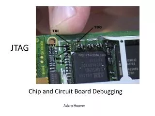
Introduction • Testing and debugging large and complex SoCs are difficult because there are many different clock domains and engineers have to devise how to access the core internals and probe them. • Accordingly, efficient design-for-test (DfT) and -debug (DfD) techniques are required.
Introduction • In modular testing, a test access mechanism (TAM), which enables the exchange of test data between external pins of a chip and its embedded cores, and test wrappers, which provides an interface between a TAM and the embedded cores.
Introduction • This paper present a test wrapper and, a test and debug interface unit. • They enable data transfer between a tester/debugger and a core-under-test (CUT) or -debug (CUD) through the available NoC to facilitate test and debug.
Problem Statement • Problem 1. Most of the existing debug infrastructures use the IEEE 1149.1 serial path for scan dump. Therefore, it takes excessively long time to perform scan dump for large SoCs. • Problem 2. In order to reduce debugging time, internal data tracing buffers and debug dedicated parallel paths can be added, but area overhead due to the additional buffers and wires becomes too great.
Problem Statement • Problem 3. No matter how quickly a debug controller tries stopping the SoC right after an event occurs, it is not possible to stop the SoC instantaneously because there is a signal propagation delay from the time the debug controller detects the event and generates a clock gating signal.
Conclusion • In this paper, authors proposed a DfD technique to reuse test infrastructure and the available NoC for debugging of an NoC-based SoC. • The main benefit of using the available on-chip network are • (i) data throughput • (ii) hybrid operation that allows a core to be taken down by a tester for examination/debug while all other cores remain in functional mode.