Download
1 / 55
560 likes | 1.72k Views
15EC323E-EMBEDDED SYSTEM DESIGN. Introduction Basics of developing for embedded systems Embedded system Initialization Atmel RISC Processors Architecture, Memory Reset and interrupt functions Parallel I/O ports Timer/Counters Serial communication using UART, SPI Analog Interfaces

E N D
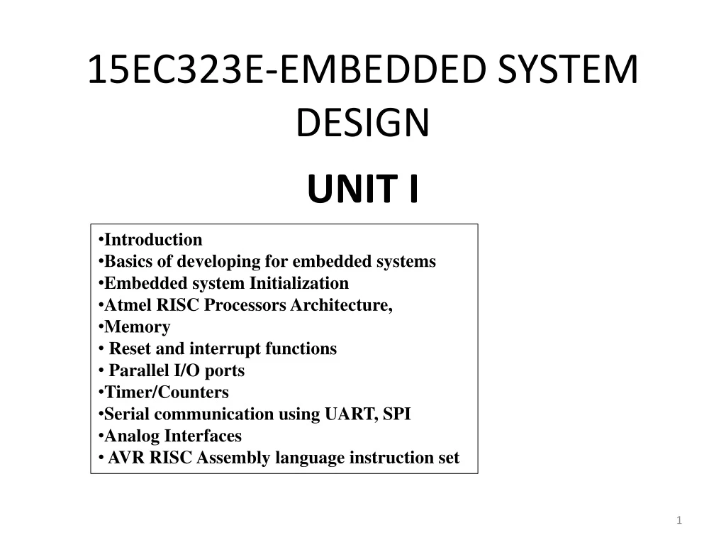
15EC323E-EMBEDDED SYSTEM DESIGN • Introduction • Basics of developing for embedded systems • Embedded system Initialization • Atmel RISC Processors Architecture, • Memory • Reset and interrupt functions • Parallel I/O ports • Timer/Counters • Serial communication using UART, SPI • Analog Interfaces • AVR RISC Assembly language instruction set UNIT I
Introduction • In ways virtually unimaginable just a few decades ago, embedded systems are reshaping the way people live, work, and play. • Embedded systems come in an endless variety of types, each exhibiting unique characteristics. • For example, most vehicles driven today embed intelligent computer chips that perform value-added tasks, which make the vehicles easier, cleaner, and more fun to drive. • Telephone systems rely on multiple integrated hardware and software systems to connect people around the world. Even private homes are being filled with intelligent appliances and integrated systems built around embedded systems, which facilitate and enhance everyday life. • Often referred to as pervasive or ubiquitous computers, embedded systems represent a class of dedicated computer systems designed for specific purposes. • Many of these embedded systems are reliable and predictable. The devices that embed them are convenient, user-friendly, and dependable. • One special class of embedded systems is distinguished from the rest by its requirement to respond toexternal events in real time. This category is classified as the real-time embedded system.
Introduction • Embedded systems are present in many industries, including industrial automation, defense, transportation, and aerospace. • For example, NASA’s Mars Path Finder, Lockheed Martin’s missile guidance system, and the Ford automobile all contain numerous embedded systems. • Users reap the advantages without having to understand the intricacies of the technology. • Remarkably adaptable and versatile, embedded systems can be found at home, at work, and even in recreational devices. • Some of the more visible examples of embedded systems are provided below
Introduction Defining the Embedded System • A general definition of embedded systems is: embedded systems are computing systems with tightly coupled hardware and software integration, that are designed to perform a dedicated function. • The word embedded reflects the fact that these systems are usually an integral part of a larger system, known as the embedding system. Multiple embedded systems can coexist in an embedding system • Embedded Processor and Application Awareness • The processors found in common personal computers (PC) are general-purpose or universal processors. They are complex in design because these processors provide a full scale of features and a wide spectrum of functionalities. • They are designed to be suitable for a variety of applications. These processors result in large power consumption, heat production, and size. • The embedded processors are special-purpose processors designed for a specific class of applications. The key is application awareness, i.e., knowing the nature of the applications and meeting the requirement for those applications that it is designed to run. • One class of embedded processors focuses on size, power consumption, and price. For example, the processor chosen for a personal digital assistant (PDA) device does not have a floating-point co-processor because floating-point operations are either not needed or software emulation is sufficient. • This class of embedded processors is small because the overall PDA device is slim and fits in the palm of your hand. • The limited functionality means reduced power consumption and long-lasting battery life. The smaller size reduces the overall cost of processor fabrication.
Introduction • Embedded Processor and Application Awareness • Another class of embedded processors focuses on performance. • These embedded processors are powerful and packed with advanced chip-design technologies, such as advanced pipeline and parallel processing architecture. • Yet another class of embedded processors focuses on all four requirements—performance, size, power consumption, and price. Take, for example, the embedded digital signal processor (DSP) used in cell phones. Real-time voice communication involves digital signal processing and cannot tolerate delays. • A DSP has specialized arithmetic units, optimized design in the memory, and addressing and bus architectures with multiprocessing capability that allow the DSP to perform complex calculations extremely fast in real time. • System-on-a-chip (SoC) processors are especially attractive for embedded systems. • The SoC processor is comprised of a CPU core with built-in peripheral modules, such as a programmable general-purpose timer, programmable interrupt controller, DMA controller, and possibly Ethernet interfaces. Such a self-contained design allows these embedded processors to be used to build a variety of embedded applications without needing additional external peripheral devices, again reducing the overall cost and size of the final product.
Introduction • Hardware and Software Co-Design Model • Commonly both the hardware and the software for an embedded system are developed in parallel. • The software component can take advantage of special hardware features to gain performanceand the hardware component can simplify module design if functionality can be achieved in software that reduces overall hardware complexity and cost. • Often design flaws, in both the hardware and software, are uncovered during this close collaboration. • Cross-Platform Development • Another typical characteristic of embedded systems is its method of software development, called cross-platform development, for both system and application software. • Software for an embedded system is developed on one platform but runs on another. In this context, the platform is the combination of hardware (such as particular type of processor), operating system, and software development tools used for further development. • The host system is the system on which the embedded software is developed. The target system is the embedded system under development. • The main software tool that makes cross-platform development possible is a cross compiler. • Across compiler is a compiler that runs on one type of processor architecture but produces object code for a different type of processor architecture. A cross compiler is used because the target system cannot host its own compiler.
Introduction • Software Storage and Upgradeability • Code for embedded systems (such as the real-time embedded operating system, the system software, and the application software) is commonly stored in ROM and NVRAM memory devices. • Upgrading an embedded system can mean building new PROM, deploying special equipment and/or a special method to reprogram the EPROM, or reprogramming the flash memory. • The choice of the storage device can also have an impact on the overall cost of maintenance. • Real-Time Embedded Systems • Real-time systems are defined as those systems in which the overall correctness of the system depends on both the functional correctness and the timing correctness. • A hard real-time system is a real-time system that must meet its deadlines with a near-zero degree of flexibility. The deadlines must be met, or catastrophes occur. • A soft real-time system is a real-time system that must meet its deadlines but with a degree of flexibility. The deadlines can contain varying levels of tolerance, average timing deadlines etc
Basics Of Developing For Embedded Systems • One characteristic of embedded systems is the cross-platform development methodology. The primary components in the development environment are the host system, the target embedded system, and potentially many connectivity solutions available between the host and the target embedded system as shown in Figure. • The essential development tools offered by the host system are the cross compiler, linker, and source-level debugger. • The target embedded system might offer a dynamic loader, a link loader, a monitor, and a debug agent. • A set of connections might be available between the host and the target system. These connections are used for downloading program images from the host system to the target system. • These connections can also be used for transmitting debugger information between the host debugger and the target debug agent. • The goal is to offer the embedded developer practical insights on how the components relate to one another. Knowing the big picture allows an embedded developer to put it all together and ask the specific questions if and when necessary. Figure 1: Typical cross-platform development environment.
Basics Of Developing For Embedded Systems • Programs including the system software, the real-time operating system (RTOS), the kernel, and the application code must be developed first, compiled into object code, and linked together into an executable image. • Programmers writing applications that execute in the same environment as used for development, called native development, do not need to be concerned with how an executable image is loaded into memory and how execution control is transferred to the application. • Embedded developers doing cross-platform development, however, are required to understand the target system fully, how to store the program image on the target embedded system, how and where to load the program image during runtime, and how to develop and debug the system iteratively. • Each of these aspects can impact how the code is developed, compiled, and most importantly linked. • The areas of focus are • the ELF object file format, • the linker and linker command file, and • mapping the executable image onto the target embedded system.
Basics Of Developing For Embedded Systems • Overview of Linkers and the Linking Process Figure below illustrates how different tools take various input files and generate appropriate output files to ultimately be used in building an executable image. • Figure:Creating an image file for the target system.
Basics Of Developing For Embedded Systems The developer writes the program in the C/C++ source files and header files. Some parts of the program can be written in assembly language and are produced in the corresponding assembly source files. The developer creates a makefile for the make utility to facilitate an environment that can easily track the file modifications and invoke the compiler and the assembler to rebuild the source files when necessary. From these source files, the compiler and the assembler produce object files that contain both machine binary code and program data. The archive utility concatenates a collection of object files to form a library. The linker takes these object files as input and produces either an executable image or an object file that can be used for additional linking with other object files. The linker command file instructs the linker on how to combine the object files and where to place the binary code and data in the target embedded system. The main function of the linker is to combine multiple object files into a larger relocatable object file, a shared object file, or a final executable image. In a typical program, a section of code in one source file can reference variables defined in another source file. A function in one source file can call a function in another source file. The global variables and non-static functions are commonly referred to as global symbols.
Basics Of Developing For Embedded Systems • In source files, these symbols have various names, for example, a global variable called foo_bar or a global function called func_a. • In the final executable binary image, a symbol refers to an address location in memory. The content of this memory location is either data for variables or executable code for functions. • The compiler creates a symbol table containing the symbol name to address mappings as part of the object file it produces. • When creating relocatable output, the compiler generates the address that, for each symbol, is relative to the file being compiled. • Consequently, these addresses are generated with respect to offset 0. • The symbol table contains the global symbols defined in the file being compiled, as well as the external symbols referenced in the file that the linker needs to resolve. • The linking process performed by the linker involves symbol resolution and symbol relocation.
Basics Of Developing For Embedded Systems Symbol resolutionis the process in which the linker goes through each object file and determines, for the object file, in which (other) object file or files the external symbols are defined. Sometimes the linker must process the list of object files multiple times while trying to resolve all of the external symbols. When external symbols are defined in a static library, the linker copies the object files from the library and writes them into the final image. Symbol relocationis the process in which the linker maps a symbol reference to its definition. The linker modifies the machine code of the linked object files so that code references to the symbols reflect the actual addresses assigned to these symbols. For many symbols, the relative offsets change after multiple object files are merged. Symbol relocation requires code modification because the linker adjusts the machine code referencing these symbols to reflect their finalized addresses. The relocation table tells the linker where in the program code to apply the relocation action. Each entry in the relocation table contains a reference to the symbol table. Using this reference, the linker can retrieve the actual address of the symbol and apply it to the program location as specified by the relocation entry. It is possible for the relocation table to contain both the address of the symbol and the information on the relocation entry. In this case, there is no reference between the relocation table and the symbol table.
Basics Of Developing For Embedded Systems • For an executable image, all external symbols must be resolved so that each symbol has an absolute memory address because an executable image is ready for execution. • The exception to this rule is that those symbols defined in shared libraries may still contain relative addresses, which are resolved at runtime (dynamic linking). • Linking is often referred to as a process that is performed when the executable is compiled, while a dynamic linker is a special part of an operating system that loads external shared libraries into a running process and then binds those shared libraries dynamically to the running process. This approach is also called dynamic linking or late linking. • A relocatable object file may contain unresolved external symbols. • Similar to a library, a linker-reproduced relocatable object file is a concatenation of multiple object files with one main difference—the file is partially resolved and is used for further linking with other object files to create an executable image or a shared object file. • A shared object file has dual purposes. It can be used to link with other shared object files or relocatable object modules, or it can be used as an executable image with dynamic linking.
Executable and Linking Format Typically an object file contains • general information about the object file, such as file size, binary code and data size, and source file name from which it was created, • machine-architecture-specific binary instructions and data • symbol table and the symbol relocation table, and • debug information, which the debugger uses. The manner in which this information is organized in the object file is the object file format. Two common object file formats are the Common Object File Format (COFF) and the Executable and Linking Format (ELF). Using the ELF object file format, the compiler organizes the compiled program into various system-defined, as well as user-defined, content groupings called sections. The program's binary instructions, binary data, symbol table, relocation table, and debug information are organized and contained in various sections. Each section has a type. Content is placed into a section if the section type matches the type of the content being stored The ELF file format has two different interpretations, as shown in Figure . The linker interprets the file as a linkable module described by the section header table, while the loader interprets the file as an executable module described by the program header table.
Basics Of Developing For Embedded Systems • A section header table is an array of section header structures describing the sections of an object file. • A program header table is an array of program header structures describing a loadable segment of an image that allows the loader to prepare the image for execution. • Program headers are applied only to executable images and shared object files. • One of the fields in the section header structure is sh_type, which specifies the type of a section. • Table lists some section types Other common system-defined sections are .symtab containing the symbol table, .strtab containing the string table for the program symbols, .shstrtab containing the string table for the section names, and .relanamecontaining the relocation information for the section named name.
Basics Of Developing For Embedded Systems The sh_flags field in the section header specifies the attribute of a section. The following are some of these attributes. WRITE Section contains writeable data. ALLOC Section contains allocated data. EXECINSTR Section containsexecutable instructions • Some common system-created default sections with predefined names for the PROGBITS are .text, .sdata, .data, .sbss, and .bss. • Program code and constant data are contained in the .textsection. This section is read-only because code and constant data are not expected to change during the lifetime of the program execution. • The .sbss and .bsssections contain uninitialized data. The .sbsssection stores small data, which is the data such as variables with sizes that fit into a specific size. This size limit is architecture-dependent. The result is that the compiler and the assembler can generate smaller and more efficient code to access these data items. • The .sdataand .data sections contain initialized data items. The small data concept described for .sbssapplies to .sdata. • A .text section with executable code has the EXECINSTR attribute. • The .sdata and .data sections have the WRITE attribute. • The .sbss and .bsssections have both the WRITE and the ALLOC attributes
Mapping Executable Images into Target Embedded Systems • Merge the sections from the different object files into program segments. • This process creates a single executable image for the target embedded system using linker directives kept in the linker command file. • The MEMORY directive can be used to describe the target systems memory map. The memory map lists the different types of memory (such as RAM, ROM, and flash) that are present on the target system.
Mapping Executable Images • Module Upgradeability • Memory Size Limitation • Data Protection • A target system has 256 bytes of ROM, 16KB of flash memory, and two blocks of RAM RAMB0 is 128KB of SDRAM, and RAMB1 is 2MB of DRAM. • Embedded application:
Embedded System Initialization • how to load the image onto the target system,· • where in memory to load the image,· • how to initiate program execution, • how the program produces recognizable output. • After the final image is successfully built and residing on the host system, the next step is to execute it on the target. • image transfer from the host to the target system, • the embedded monitor and debug agent, • the target system loader, • the embedded system booting process, • various initialization procedures. • An executable image built for a target embedded system can be transferred from the host development system onto the target, which is called loading the image, by: • Programming the entire image into the EEPROM or flash memory. • Downloading the image over either a serial (typically RS-232) or network connection. This process requiresthe presence of a data transfer utility program on the host system, as well as the presence of a target loader,an embedded monitor, or a target debug agent on the target system.· • Downloading the image through either a JTAG or BDM interface
Target System Tools and Image Transfer • The entire executable image is burned into the ROM or flash memory using special equipment. • For embedded system boards that have both ROM and flash memory, the next step is to set the necessary jumpers. • Jumpers are the part of the target board's wiring that controls, which memory chip the processor uses to start executing its first set of instructions upon reboot.
Target System Tools and Image Transfer Embedded Loader: A common approach taken at the early development phase is to write a loader program for the target side, which is called the loader, and use the loader to download the image from the host system. Embedded Monitor: A monitor is an embedded software application commonly provided by the target system manufacturer for its evaluation boards. The monitor enables developers to examine and debug the target system at run time. The monitor is generally developed by the hardware engineers and is also used by the hardware engineers to perform both system device diagnostics and low-level code debugging Target Debug Agent: The target debug agent functions much like the monitor does but with one added feature: the target agent gives the host debugger enough information to provide visual source-level debug capability
Target Boot Scenarios • Embedded processors, after they are powered on, fetch and execute code from a predefined and hard-wired address offset. • The code contained at this memory location is called the reset vector. The reset vector is usually a jump instruction into another part of the memory space where the real initialization code is found. • The reason for jumping to another part of memory is to keep the reset vector small. The reset vector belongs to a small range of memory space reserved by the system for special purposes. • The reset vector, as well as the system boot startup code, must be in permanent storage. • The system startup code, called the bootstrap code, resides in the system ROM, the on-board flash memory, or other types of non-volatile memory devices.
Target Boot Scenarios Executing from ROM Using RAM for Data Executing from RAM after Image Transfer from ROM Executing from RAM after Image Transfer from Host
Target Boot Scenarios Executing from ROM Using RAM for Data Some embedded devices have such limited memory resources that the program image executes directly out of the ROM. Sometimes the board vendor provides the boot ROM, and the code in the boot ROM does not copy instructions out to RAM for execution. In these cases, however, the data sections must still reside in RAM. Executing from RAM after Image Transfer from ROM In the second boot scenario, the boot loader transfers an application image from ROM to RAM for execution. The large application image is stored in ROM in a compressed form to reduce the storage space required. The loader must decompress this image before it can initialize the sections of that image. During the development phase the program under construction is incomplete and is being constantly updated. As such, this program might not be able to handle certain system interrupts and exceptions. It is beneficial to have the monitor conduct default processing in such cases Executing from RAM after Image Transfer from Host In the third boot scenario, the target debug agent transfers an application image from the host system into RAM for execution. This practice is typical during the later development phases when the majority of the device drivers have been fully implemented and debugged. The system can handle interrupts and exceptions correctly.
Target System Software Initialization Sequence Hardware Initialization 1.starting execution at the reset vector 2.putting the processor into a known state by setting the appropriate registers: getting the processor type ,getting or setting the CPU s clock speed 3.disabling interrupts and caches 4.initializing memory controller, memory chips, and cache units: getting the start addresses for memory, getting the size of memory, performing preliminary memory tests, if required 5. setting up execution handlers; 6. initializing interrupt handlers; 7. initializing bus interfaces, such as VME, PCI, and USB; and 8. initializing board peripherals such as serial, LAN, and SCSI. RTOS Initialization 1.initializing the RTOS 2.initializing different RTOS objects and services, if present (usually controlled with a user-configurable header file, task objects, semaphore objects, message-queue objects, timer services, interrupt services, memory-management services 3. creating necessary stacks for RTOS 4.initializing additional RTOS extensions, such as: TCP/IP stack, file systems 5. starting the RTOS and its initial tasks • Application Software Initialization • After the RTOS is initialized and running with the required components, control is transferred to a user-defined application. • This transfer takes place when the RTOS code calls a predefined function (that is RTOS dependent)which is implemented by the user-defined application
On-Chip Debugging(OCD) JTAG stands for Joint Test Action Group, which was founded by electronics manufacturers to develop a new and cost-effective test solution. The result, produced by the JTAG consortium, is sanctioned by the IEEE1149.1 standard. BDM stands for Background Debug Mode. It refers to the microprocessor debug inter- face introduced by Motorola and found on its processor chips. The term also describes the non-intrusive nature (on the executing system) of the debug method provided by the OCD solutions.
AT90S/LS8535 Features : • Utilizes the AVR Enhanced RISC Architecture • AVR - High Performance and Low Power RISC Architecture • 118 Powerful Instructions - Most Single Clock Cycle Execution • 8K bytes of In-System Programmable Flash – SPI Serial Interface for In-System Programming • 512 bytes EEPROM • 512 bytes Internal SRAM • 8-Channel, 10-Bit ADC • 32 x 8 General Purpose Working Registers • 32 Programmable I/O Lines (PORT A,B,C,D) • Programmable Serial UART • Speed Grades: 0 - 8 MHz • RTC with Separate Oscillator and Counter Mode • Two 8-Bit Timer/Counters with Separate Prescaler and Compare Mode • One 16-Bit Timer/Counter with Separate Prescaler and Compare and Capture Modes • 3 PWM channels • External and Internal Interrupt Sources • Programmable Watchdog Timer with On-Chip Oscillator • On-Chip Analog Comparator • Three Sleep Modes: Idle, Power Save, and Power Down • Programming Lock for Software Security
ARCHITECTURE • The AVR core combines a rich instruction set with 32 general purpose working registers. • All the 32 registers are directly connected to the Arithmetic Logic Unit (ALU), allowing two independent registers to be accessed in one single instruction executed in one clock cycle. • The resulting architecture is more code efficient while achieving throughputs up to ten times faster than conventional CISC microcontrollers. • Three Sleep Modes: Idle, Power Save, and Power Down • The Idle mode stops the CPU while allowing the SRAM, timer/counters, SPI port and interrupt system to continue functioning. • The Power Down mode saves the register contents but freezes the oscillator, disabling all other chip functions until the next interrupt or hardware reset. • In Power Save mode, the timer oscillator continues to run, allowing the user to maintain a timer base while the rest of the device is sleeping.
PARALLEL PORTS Port A (PA7..PA0) Port A is an 8-bit bi-directional I/O port. Port pins can provide internal pull-up resistors (selected for each bit). The Port A output buffers can sink 20mA and can drive LED displays directly. When pins PA0 to PA7 are used as inputs and are externally pulled low, they will source current if the internal pull-up resistors are activated. Port A also serves as the analog inputs to the A/D Converter. Port B (PB7..PB0) Port B is an 8-bit bi-directional I/O pins with internal pull-up resistors. The Port B output buffers can sink 20 mA. As inputs, Port B pins that are externally pulled low will source current if the pull-up resistors are activated. Port C (PC7..PC0) Port C is an 8-bit bi-directional I/O port with internal pull-up resistors. The Port C output buffers can sink 20 mA. As inputs, Port C pins that are externally pulled low will source current if the pull-up resistors are activated. Two Port C pins can alternatively be used as oscillator for Timer/Counter2. Port D (PD7..PD0) Port D is an 8-bit bidirectional I/O port with internal pull-up resistors. The Port D output buffers can sink 20 mA. As inputs, Port D pins that are externally pulled low will source current if the pull-up resistors are activated.
TIMERS Timer 0 is typically an 8-bit timer, but this varies by specific processor type. It is capable of the usual timer/counter functions but is most often used to create a time base or tick for the program. Timer counter control register 0, TCCR0, controls the function of Timer 0 by selecting the clock source applied to Timer 0. TCCR0 Prescaler Definitions
TIMERS Timer 1 is controlled through a control register. Timer/counter control register 1, TCCR1 is actually composed of two registers,TCCR1A and TCCR1B. TCCR1A controls the compare modes and the pulse width modulation modes of Timer 1. TCCR1B controls the prescaler and input multiplexer for Timer 1, as well as the input capture modes. WGM- Waveform Generation Mode (Normal, PWM –Phase correct, CTC(Clear Timer on Compare), Fast PWM) FOC – Force Output Compare(1-immediate compare )
TIMERS • Timer 1 Input Capture Mode • To measure an event, the time on Timer 1 is captured or held at the beginning of the event, the time is also captured at the end of the event, and the two are subtracted to find the time that it took for the event to occur. • ICR1 is a 16-bit register (made up of ICR1H and ICR1L) that will capture the actual reading of Timer 1 when the microcontroller receives a certain signal. • The signal that causes a capture to occur can be either a rising or a falling edge applied to the input capture pin, ICP, of the microcontroller. • Timer 1 Output Compare Mode • In output compare mode, the program loads an output compare register. The value in the output compare register is compared to the value in the timer/counter register, and an interrupt occurs when the two values match. • Two 16 bit output compare registers are available for compare operation (OCR1A & OCR1B)
TIMERS • Timer 1 Pulse Width Modulator Mode • Pulse width modulation (PWM) mode is one of a number of methods of providing digital to analog conversion. • PWM is the scheme in which the duty cycle of a square wave output from the microcontroller is varied to provide a varying DC output by filtering the actual output waveform to get the average DC • The actual duty cycle being output in PWM mode depends on the value loaded into the output compare register for the timer/counter
TIMERS • Timer 2 • Timer 2 is usually an 8-bit timer/counter with output compare and PWM features similar to Timer 1. • The most interesting difference with Timer 2 is that it can use a crystal separate from the system clock as its clock source. • Selection of the external crystal as the clock source for Timer 2 is accomplished by setting the AS2 bit in the asynchronous status register (ASSR). • AS = 0 –system clock; AS=1 – Asynchronous clock • TCN2UB – Timer/Counter 2 Update busy – 0 = ready for new i/p, 1= busy • OCR2UB – Output compare register update busy • TCR2UB – Timer/counter Control register update busy
SERIAL COMMUNICATION-UART • Serial communication is the process of sending multiple bits of data over a single wire. • Asynchronous serial communication uses a start bit and a stop bit added to the data byte to allow the receiver to determine the timing of each bit • The only issue confronting the programmer is to ensure that the serial communication parameters of both the transmitter and the receiver match, like setting the correct number of data bits (usually 8), determining whether or not to include a parity bit (usually not), and setting the baud rate. • The baud rate is the speed of serial communication and determines the timing of the bits. • Baud rate is defined as the inverse of the time per bit (baud rate = 1/bit time).
SERIAL COMMUNICATION-UART • The USART interface consists of three registers. These are the USART control and status Register , a 16-bit register consisting of two 8-bit registers, UCSRA and UCSRB, the USART baud rate register, a 16-bit register consisting of UBRRH and UBRRL, and the USART data register. • UDR is actually two registers sharing a single I/O address. One is a read-only register and one is a write-only register. The read-only register contains any serial byte received, and the write-only register contains any serial byte to be transmitted. • For other modes of operation an additional UART control and status register, UCSRC, is used
SERIAL COMMUNICATION-UART URSEL – USART Register Select UMSEL – USART Mode Select UPM1:0 – Parity Mode USBS – Stop Bit Select • UCSZ1:0 – Character Size • UCPOL – Clock Polarity UBRR = (System Clock / (16 * baudrate)) – 1
SERIAL COMMUNICATION-SPI • Serial Peripheral Interface, SPI is a synchronous serial communication bus, meaning that the transmitter and receiver involved in SPI communication must use the same clock to synchronize the detection of the bits at the receiver • Used for very short distance communication with peripherals or other microcontrollers that are located on the same circuit board or at least within the same piece of hardware • The SPI bus was developed to provide relatively high-speed, short distance communication using a minimum number of microcontroller pins. • SPI communication involves a master and a slave. Both the master and a slave send and receive data simultaneously, but the master is responsible for providing the clock signal for the data transfer. • In this way, the master has control of the speed of data transfer and is, therefore, in control of the data transfer
SERIAL COMMUNICATION-SPI master-out-slave-in (MOSI)-master to slave master-in-slave-out (MISO)-slave to master