Download
1 / 13
130 likes | 241 Views
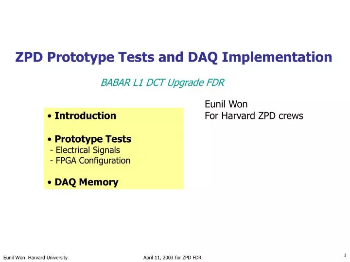
ZPD Prototype Tests and DAQ Implementation. BABAR L1 DCT Upgrade FDR. Eunil Won For Harvard ZPD crews. Introduction Prototype Tests - Electrical Signals - FPGA Configuration DAQ Memory. Printed Circuit Board. Two prototypes were assembled (May 2002)

E N D
ZPD Prototype Tests and DAQ Implementation BABAR L1 DCT Upgrade FDR Eunil Won For Harvard ZPD crews • Introduction • Prototype Tests • - Electrical Signals • - FPGA Configuration • DAQ Memory
Printed Circuit Board • Two prototypeswere assembled(May 2002) • Power connection viasunconnectedin PCB(Layout software bug) • - Extra wires jumped for prototypes • Clock Signals on Decoder Driver routed incorrectly to normal I/O • - To be fixed in the production version • One arrived at SLAC (July 2002) power on : no smoke and it booted successfully!
Flow of Signals in ZPD “Megabus” (74:0) Segments (152:0) 60 MHz 120 MHz Six Algorithm Engines Frame (8:0) J1 Algorithm Engine Algorithm Engine Decoder Driver Segments(152:0) J2 Decision Module “Minibus” (15:0) : memory access Decision (7:0) 30 MHz 8 MHz C/D link Fit Results (11:0) x 6 :to Decision Module J3 C/D clock 30 MHz Not shown: signals to LEDs, Logic Analyzer ports…
Prototype Testing • Testing prototype boards involve • PCB level tests • Does it boot? • All signals are connected? • Crosstalk (in segments/Megabus)? • Firmware level tests • Fast Control commands functional? • Memory read/write OK? • Algorithm works/fits?(Stephen’s talk) Two crucial steps toward production
Testing Signals From ZPDi to ZPD (Decoder Driver) : 60 MHz Test Patterns from ZPDi Frame bit Segment (152:0) Decoder Driver Segment # Diagnostic Memory J1 / J2 Record segment patterns into memory and check contents… (Automatically involves partial test of fast control and memories) Tested up to 10^10 bits/trace and no errors found (limited by software speed)
Testing Signals From Decoder Driver to Algorithm Engines (“The Megabus Test”) : 120 MHz Six Algorithm Engines Megabus (74:0) Algorithm Engine Algorithm Engine Decoder Driver • This test is one of most important (runs at 120 MHz) pieces to confirm • A dedicated firmware was written for this particular test (N. Felt @ Harvard) Up to 10^13 bits/trace with no errors Out of 75, 5 bits are reserved for future usage
Testing Signals From Algorithm Engines to Decision Module (six buses (11:0)) and Decision bits to ZPDi Algorithm Engine Algorithm Engine Six Algorithm Engines tested up to 10^6 bits/trace 30 MHz J2 Decision Module Decision bits (7:0) : 8 MHz All bits were tested with no errors
Miscellaneous • Memory access bus (“minibus”) tested with 10^8read/writes • Also Tested (partially): • 47 LEDs (front panel) • C/D clock, C/D link • L1Accept, L1Accept Buffer (1:0) • Read_Event, Read_Event Buffer (1:0) • JTAG to SystemACE, SystemACE to FPGAs • Logic Analyzer ports • Extra bus with 8 bits (reserved) connected to all FPGAs (“xbus”) All tested with no errors
Summary of PCB level Tests Two most critical items Tested “by hand”
FPGA Configuration • Prototype originally used Xilinx System ACE MPM • One-piece solution for multi-FPGA configuration • Suffered from mysterious bugs – Immature technology? • ~1 hour to reprogram ZPD 1 shift for 8 boards • Switched to System ACE CF (Compact Flash) • Flexible, inexpensive and fast to reprogram: < 20 seconds • Tested on prototype with an add-on card Great success JTAG FPGA FPGA FPGA Program
MPM Patch PCB CF card Holder FPGA Configuration : Regarding PCB changes For prototypes, the add-on goes in JTAG socket on front panel ZPD JTAG socket ZPD A small add-on of PCB Production: we will have all the patch on board (Necessary artworks etc all done)
16 bit wide Header (tag, counter, CSR) 2 words 10 words x 8 ticks TSF input mask bits (0:152) of eight CLK4 ticks Fit results (z0,dz0,r,tanl) and trigger decisions(0:7) of eight CLK4 ticks 25 words x 8 ticks DAQ Memory Decoder Driver Decision Module • In total, it amounts to 566 bytes/event/board • (cf GLT: 583 bytes/event) • Firmware written and under testing • - Bug fixes are in progress • - Tests with high rate L1 triggers need to be done
Summary • All the PCB level tests demonstrated • - • We do have modifications to make • - Fix power vias • - Correct clock routings to Decoder Driver • - Replace FPGA configuration method • DAQ Memory • - Firmware written and under testing • - Tests with high rate L1 triggers are planned No showstoppers for the production Next big hurdle: Algorithm Stephen’s Talk