Download
1 / 38
380 likes | 572 Views
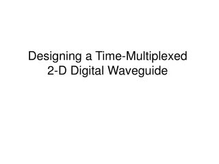
Designing a Time-Multiplexed 2-D Digital Waveguide. Simple 1D Waveguide. 210. 3. 2. 0. 0. 01. 0 21. 1. 2. 1. 0. 12. 10 2. 2. 2. 2. 0. 2 0. 210. 3. 2. 0. 01. 0. 0 21. 1. 2. 1. 0. 12. 10 2. 2. 2. 2. 0. 2 0. Note: This slide is animated – View in slide show. 210.

E N D
Simple 1D Waveguide 210 3 2 0 0 01 021 1 2 1 0 12 102 2 2 2 0 20 210 3 2 0 01 0 021 1 2 1 0 12 102 2 2 2 0 20 Note: This slide is animated – View in slide show
210 3 2 0 0 01 021 1 2 1 0 12 102 2 2 2 0 20 210 3 2 0 01 0 021 1 2 1 0 12 102 2 2 2 0 20 Time-muxed junction design
876543210 9 852 0 Simple 2D Waveguide Only left/right data communication 630 01234567 087654321 1 528 1 063 12345678 0 1 2 3 4 5 6 7 8
876543210 9 852 0 630 01234567 087654321 1 528 1 063 12345678 108765432 258 2 2 063 23456780 0 1 2 3 4 5 6 7 8
876543210 9 852 0 630 01234567 087654321 1 528 1 063 12345678 108765432 258 2 2 063 23456780 0 1 2 210876543 3 258 3 063 34567801 3 4 5 6 7 8
876543210 9 852 0 630 01234567 087654321 1 528 1 063 12345678 108765432 258 2 2 063 23456780 0 1 2 210876543 3 258 3 063 34567801 3 4 5 321087654 582 4 4 306 45678012 6 7 8
876543210 9 852 0 630 01234567 087654321 1 528 1 063 12345678 108765432 258 2 2 063 23456780 0 1 2 210876543 3 258 3 063 34567801 3 4 5 321087654 582 4 4 306 45678012 432108765 5 582 5 6 7 8 306 56780123
876543210 9 852 0 630 01234567 087654321 1 528 1 063 12345678 108765432 258 2 2 063 23456780 0 1 2 210876543 3 258 3 063 34567801 3 4 5 321087654 582 4 4 306 45678012 432108765 5 582 5 6 7 8 306 56780123 543210876 582 6 6 306 67801234
876543210 9 852 0 630 01234567 087654321 1 528 1 063 12345678 108765432 258 2 2 063 23456780 0 1 2 210876543 3 258 3 063 34567801 3 4 5 321087654 582 4 4 306 45678012 432108765 5 582 5 6 7 8 306 56780123 543210876 582 6 6 306 67801234 654321087 825 7 7 630 78012345
876543210 9 852 0 630 01234567 087654321 1 528 1 063 12345678 108765432 258 2 2 063 23456780 0 1 2 210876543 3 258 3 063 34567801 3 4 5 321087654 582 4 4 306 45678012 432108765 5 582 5 6 7 8 306 56780123 543210876 582 6 6 306 67801234 654321087 825 7 7 630 78012345 765432108 8 825 8 630 80123456
876543210 9 852 0 630 01234567 087654321 1 528 1 063 12345678 108765432 258 2 2 063 23456780 0 1 2 210876543 3 258 3 063 34567801 3 4 5 321087654 582 4 4 306 45678012 432108765 5 582 5 6 7 8 306 56780123 543210876 582 6 6 306 67801234 654321087 825 7 7 630 78012345 765432108 8 825 8 630 80123456 876543210 9 825 0 630 01234567
876543210 9 852 0 630 01234567 087654321 1 528 1 063 12345678 108765432 258 2 2 063 23456780 0 1 2 210876543 3 258 3 063 34567801 3 4 5 321087654 582 4 4 306 45678012 432108765 5 582 5 6 7 8 306 56780123 543210876 582 6 6 306 67801234 654321087 825 7 7 630 78012345 765432108 8 825 8 630 80123456 876543210 9 825 0 630 01234567 Time-muxed junction design
0 1 2 Simple 2D Waveguide Only up/down data communication 3 4 5 6 7 8 876543210 087654321 678 780 0 1 321 210 012345 123456
0 1 2 3 4 5 6 7 8 876543210 087654321 108765432 678 780 801 0 1 2 321 432 210 012345 123456 234567
0 1 2 3 4 5 6 7 8 876543210 087654321 108765432 210876543 678 780 801 012 0 1 2 3 321 432 543 210 012345 123456 234567 345678
0 1 2 3 4 5 6 7 8 876543210 087654321 108765432 210876543 321087654 678 780 801 012 012 0 1 2 3 4 321 432 543 654 210 012345 123456 234567 345678 456780
0 1 2 3 4 5 6 7 8 876543210 087654321 108765432 432108765 210876543 321087654 678 780 801 012 012 012 5 0 1 2 3 4 321 432 543 654 765 210 567801 012345 123456 234567 345678 456780
0 1 2 3 4 5 6 7 8 876543210 087654321 108765432 432108765 543210876 210876543 321087654 678 780 801 012 012 012 012 5 6 0 1 2 3 4 321 432 543 654 765 210 876 567801 678012 012345 123456 234567 345678 456780
0 1 2 3 4 5 6 7 8 876543210 087654321 108765432 432108765 543210876 654321087 210876543 321087654 678 780 801 012 012 012 012 126 7 5 6 0 1 2 3 4 321 432 543 654 765 210 876 087 567801 678012 780123 012345 123456 234567 345678 456780
0 1 2 3 4 5 6 7 8 876543210 087654321 108765432 432108765 543210876 654321087 765432108 210876543 321087654 678 780 801 012 012 012 012 126 267 7 8 5 6 0 1 2 3 4 321 432 543 654 765 210 876 087 108 567801 678012 780123 801234 012345 123456 234567 345678 456780
0 1 2 3 4 5 6 7 8 876543210 087654321 108765432 432108765 543210876 654321087 765432108 876543210 210876543 321087654 678 780 801 012 012 012 012 126 267 678 7 8 0 5 6 0 1 2 3 4 321 432 543 654 765 210 876 087 108 210 567801 678012 780123 801234 012345 012345 123456 234567 345678 456780
0 1 2 3 4 5 Time-muxed junction design 6 7 8 876543210 087654321 108765432 432108765 543210876 654321087 765432108 876543210 210876543 321087654 7 8 0 5 6 0 1 2 3 4 321 432 543 654 765 210 876 087 108 210 567801 678012 780123 801234 012345 012345 123456 234567 345678 456780 876 087 108 210 210 210 210 621 762 876
0 1 2 3 4 5 Combined time-muxed junction design incorporating both directions 6 7 8
Time-Multiplexing via C-Slowing/Retiming Simple 1D Example
0 1 2 Starting circuit
0 1 2 C-Slow by 3 (time-multiplexing factor) Label register sets 1, 2 and 3
0 1 2 Retime orange registers backwards through junction to label middle junction inputs with 1
0 1 2 Retime yellow registers backwards through junction to label righthand junction inputs with 2
0 1 2 Retime end registers so that each section looks the same
We will load only one data set into the registers labeled with a 0. The other registers are “empty” On the 0th cycle, only junction 0 has work to do. Junction 1 and 2 are idle.
After the 0th cycle, the data is now all in register set 1. On the 1th cycle, only junction 1 has work to do. Junction 0 and 2 are idle.
After the 1th cycle, the data is now all in register set 2. On the 2th cycle, only junction 2 has work to do. Junction 0 and 1 are idle.
This group on the right needs its own registers since it uses the same registers as the group on the left. We are now back to the 0th cycle where all the data is in register set 0. If you look at the registers that are used on each cycle, the three groups of registers on the left can all share a single group of registers.
Since only one junction is active each cycle, we need only one. We can share registers but need muxes to implement what happens on the different cycles.
876543210 9 852 0 630 01234567 087654321 1 528 1 063 12345678 108765432 258 2 2 063 23456780 0 1 2 210876543 3 258 3 063 34567801 3 4 5 321087654 582 4 4 306 45678012 432108765 5 582 5 6 7 8 306 56780123 543210876 582 6 6 306 67801234 654321087 825 7 7 630 78012345 765432108 8 825 8 630 80123456 876543210 9 825 0 630 01234567
0 1 2 3 4 5 6 7 8 876543210 087654321 108765432 432108765 543210876 654321087 765432108 876543210 210876543 321087654 678 780 801 012 012 012 012 126 267 678 7 8 0 5 6 0 1 2 3 4 321 432 543 654 765 210 876 087 108 210 567801 678012 780123 801234 012345 012345 123456 234567 345678 456780