Download
1 / 12
120 likes | 236 Views
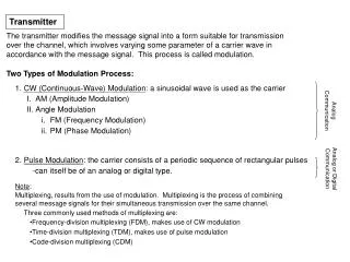
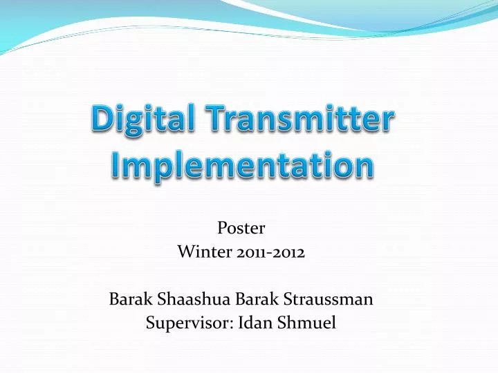
Digital Transmitter Implementation. Poster Winter 2011-2012 Barak Shaashua Barak Straussman Supervisor: Idan Shmuel. Project Goals. Implementation of a transmitter with Labview on FPGA . Project modulation types: 4 DQAM 8 DPSK. Hardware Connection.

E N D
Digital Transmitter Implementation Poster Winter 2011-2012 Barak Shaashua Barak Straussman Supervisor: IdanShmuel
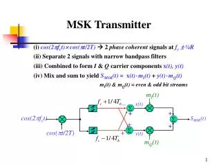
Project Goals • Implementation of a transmitter with Labview on FPGA. • Project modulation types: • 4 DQAM • 8 DPSK
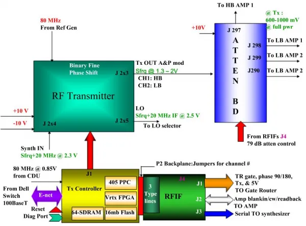
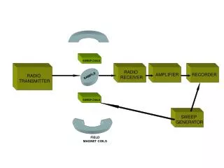
Hardware Connection NI 5761 Digitizer + NI FlexRioFPGA 7965R as RX NI FlexRioFPGA 7965R as TX • Tabor – wx2182 as DAC 2.1GS/s 250MS/s 16MB memory 1.5MB/s
System Problems • The bottleneck of the system is the speed of the DAC (Tabor wx2182) connection through the GPIB cable. • Therefore, the system complexity was reduced by simulating The TX on the HOST. (Even though the TX works on the FPGA). • Streaming is not supported by the DAC through the GPIB. Transmission is done in packets as big as the memory of the DAC. • The DAC doesn’t transmit both channels synchronically (without trigger). • As a result, the two channels are combined on the HOST and delivered to the DAC as one channel.
Data Rates • Transmitter boundary: DAC max sample rate: 2.1GS/sec. In this rate carrier wave frequency: 1.05GHz. • Receiver boundary: The ADC (NI5761) - max sample rate: 250MS/sec --> BW = 125MHz. • Data boundary: Limited by the DAC memory size - 16M samples.
Transmitter Block Diagram I Source Coder Channel Coder Serial / Parallel Constellation Mapping Q DAC I + π/2 ISI Filter Up Converter Combiner Q Sin(wt) DAC
Receiver Block-Diagram LPF I Timing & Carrier Recovery + π/2 ADC RF Sin(wt) Q LPF I Channel Decoder Symbol Decision Constellation Mapping Parallel / Serial Q (+ Source)
Transmission Parameters • We worked with Carrier frequency: 50MHz + 10 samples per period --> DAC operates in 500MS/sec. • Symbol = 1 period of the carrier. • Data rate: DQPSK - 2 bit/symbol - 100Mbit/sec. D8PSK - 3 bit/symbol - 150Mbit/sec. • With 16M DAC memory - Data transition per transmission: 400KB (DQPSK) / 600KB (D8PSK).
Results • 25MHz transmission --> BER=0 (One symbol error at the edge, not dependent on transmission length) • 50MHz transmission --> BER=0 • 80MHz transmission --> BER=1/3 • No alignment between samples and carried periods. • Over sampling too low.
Summery • In this project we acquired a lot of knowledge about communication and modulation. • The project involved the integration of variety of systems and work environments. • Future improvements: • Labview - We found it hard to debug FPGA VI. • Tabor - In our project setting, wx2182 wasn’t suitable.