Download
1 / 20
230 likes | 288 Views
OVONIC UNIFIED MEMORY. Submitted by Kirthi K Raman 4PA06EC044 Under the guidance of Prof. John Valder

E N D
OVONIC UNIFIED MEMORY Submitted by Kirthi K Raman 4PA06EC044 Under the guidance of Prof. John Valder P A College of Engg
CONTENTS • Introduction • Present Memory Technology Scenario • Emerging Memory Technologies • Ovonic Unified Memory • OUM Attributes • OUM Architecture • Integration with Cmos • Circuit Demonstration • Advantages • Conclusion • Reference
Introduction • Semiconductors form the fundamental building block of the modern electronic world. • Scaling of CMOS IC Technology faces uphill technology challenge. • For digital application, challenges include exponentially increasing leakage current, short channel effects , etc. • For RF application, challenges include low noise figure, sustained linearity ,transistor matching, power added efficiency, etc.
PRESENT MEMORY TECHNOLOGY SCENARIO Limitations • DRAM is volatile and difficult to integrate. • RAM is expensive and volatile. • Flash has slower writes and lesser number of write/erase cycle compared to others. • These memory technologies when expanded allows expansion only in 2D . • Hence large area is required.
EMERGING MEMORY TECHNOLOGY • Emerging memory technologies are called Next Generation Memories. • Most important property of these NGM is its ability to support expansion in 3Dspace. • NGM include NRAM, FeRAM, Polymer Memory Ovonic Unified Memory, ETOX, NRAM ,etc.
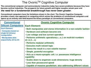
OVONIC UNIFIED MEMORY 1.OUM is a non volatile memory, which uses chalcogenide materials for storage of binary data. 2.OUM uses reversible structural phase change. amorphous phase crystalline phase . 3. Resistive property of the phases is used to represent 0s and 1s.
OUM Technology Concept Amorphous Vs Crystalline Short Range Atomic Order Low Free Electron Density High Activation Energy High Resistivity Long Range Atomic Order High Free Electron Density Low Activation Energy Low Resistivity
(ten minute isochronal anneal) OUM Technology Concept Annealing Dependence of Ge2Sb2Te5 Electrical Resistivity
OUM Attributes • density ensures large storage of data within a small area. Non volatile in nature. • High • Non destructive read • Uses very voltage and power from a source. • Write/erase cycles of 10e12 demonstrated • Poly Crystalline • Offers the potential of easy addition of non volatile memory to a standard CMOS processor • Highly scalable memory • Low cost implementation
Circuit Demonstration • Chalcogenide Technology Characterization Vehicle (CTCV) • Key goals in the design of CTCV 1. To make the read and write circuit wrt variation in cell electrical characteristics 2. To test the effect of the memory cell layout on performance 3. To maximize the amount of useful data obtained , used for product design.
One of the Chiplet used fig Conservative FET Cell Single Ended Sense Amp Aggressive FET Cell Single Ended Sense Amp Conservative FET Cell Differential Sense Amp Aggressive FET Cell Differential Sense Amp Process Monitor Circuits
Advantages • OUM uses a reversible structural phase change • Cost/Bit reduction • small active storage medium • small cell size-small die size • Simple manufacturing process • Simple planar device structure • Low voltage-single supply • Reduced assembly and test costs • Highly scalable • Performance improves with scaling • Only lithography limited • Low voltage operation • Multi state demonstrated
Risk Factors • Reset current< min W switch current • Standand CMOS process integration • Alloy optimization for robust high temp operation and speed • Cycle life endurance consistency • Endurance testing to 1014-DRAM • Defect density and failure mechanisms
Conclusion • Near ideal memory qualities • Broadens system application -Embedded System-On-a-Chip(SOC) , other products • Highly Scalable • Risk factors have been identified • Time to productize
References • www.intel.com • www.ovonyx.com • www.baesystems.com • www.aero.org • IEEE SPECTRUM, March 2003