Download
1 / 61
610 likes | 612 Views
This agenda includes an introduction to RF design, a case study of a power amplifier design, and measurement techniques for design verification. The focus is on designing for maximum power output, matching to the FET output, and refining the design for stability.

E N D
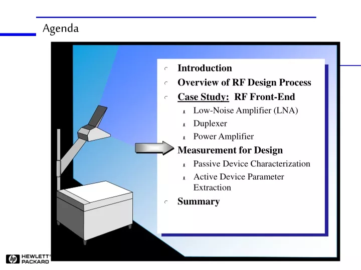
Agenda • Introduction • Overview of RF Design Process • Case Study: RF Front-End • Low-Noise Amplifier (LNA) • Duplexer • Power Amplifier • Measurement for Design • Passive Device Characterization • Active Device Parameter Extraction • Summary
Power Amp Design 1.88 GHz PCS-Band Amplifier • Gain > +24 dB • 1-dB-compression > +25 dBm • Psat > +27 dBm Main challenge: designing for maximum power output During brainstorm process, decided: • two stages needed to get desired gain • stage one: • silicon transistor • passive bias • stage two: • power FET • active bias power stage driver stage
Bias Considerations - Active vs. Passive • passive - simpler, less space, cheaper but not as well controlled • active - extra circuitry, but more repeatable • hint: watch out for over-biasing junctions (FET gate-bias example) changed to -6V to prevent gate over-voltage condition
S 22 Designing the Output Stage for Maximum Output Power • output impedance varies as function of output power • ideal impedance exists for maximum output power • two technique provides information for output-stage matching • load-pull technique • load-line analysis Low power High power
Pmax -1dB -2dB -3dB DUT Load-Pull Technique • vary magnitude and phase of load presented to circuit • power output is measured at each impedance point • can use behavioral model (based on measurements) Output impedance and power measurement system Input impedance and power measurement system X X X X Input Tuner Output Tuner Constant output power contours versus output load impedance (input power constant) Can be very expensive and time-intensive
1.3 x 600 mA = 780 mA useable region Id 1.3 Idss Load line = (16.5 - 1.5) .780 = 19.2 ohms = RL useable region Po = (Ipk / 2Ö2) x RL = 1.44 W = +31.6 dBm 2 Vds 9 + (9 - 1.5) = 16.5 V maximum 1.5 V minimum 9 V nominal Load-Line Analysis • determines resistance that gives highest power • current source of FET needs to be presented with this load • should give same output match as load-pull technique
Matching to FET Output Output match of FET chip • need to have accurate physical model of device • parasitics must be included in matching circuit • include FET and package parasitics • assume simple parallel-output capacitance for FET • can determine Cp from chip model • use mirror-matching technique M1 external output matching circuit Package model Ouput capacitance of FET Load resistor determined from load-line analysis match to 50 ohms here Id = Vgate x gm + Vgate Co - Co = y / (2pf * 50) = 1.02 pf
L R Load-Pull Simulation - 6 dB contour - 5 dB contour - 4 dB contour - 3 dB contour - 2 dB contour Pmax ( 32.4 + j 35.7 ) - 1 dB contour Simpler, Faster, and Far less expensive our designed impedance ( 42.15 + j 23.45 )
Using data from the load-pull simulation to design a matching network • No need to model parasitics of FET or package • Use mirror-matching technique • Easier and faster Conjugate match of load impedance external output matching circuit - j 23.45 42.15 ohms match to 50 ohms here
Measured Performance of First Prototype CH1 S log MAG 10 dB/ REF 30 dB 21 * 1_: 1.641 GHz 30.39 dB PRm 2_: 1.880 GHz 17.584 dB 3 Cor 3_: 651.419 MHz 40.93 dB Avg measured 0 simulated (entire amp) 1 Hld 2 simulated (preamp only) START 100.000 000 MHz STOP 3 000.000 000 MHz
Modifying Tips First, verify there are no errors in the fabrication or measurement of the prototype. Why modify the circuit design file to match the prototype? Because a prototype is a very useful tool for improving the accuracy of the circuit design file gives good assurance that design changes will indeed improve design Can start by, - accounting for fringing effects or discontinuities - removing transistor and measuring only bias components - connecting ground vias directly to the main transmission line
m1= 650 MHz New capacitor models Measured Old capacitor models Modify the circuit design file
s-para file Importance of accurate measurements Desired reference plane (A) (B) (C) (D) Reference plane, set by test fixture calibration Reference plane of capacitor’s measured s-parameter Desired reference plane of capacitor’s measured s-parameter test fixture (additional transmission line lengths, 20 mils on either side) Modified s-parameter model of capacitor
Design Refinement driver stage power stage s11 s22 2 gain stages, oscillation can be caused by: .. driver stage .. power stage .. both stages ----> Need to separate each stage and examine
Driver Stage Gain Stability Circles
Power Stage: Input & Output Match Potentially Unstable
Schematic of New Power Stage trap feedback loop
Completed amplifier’s s11 and s22 responses with duplexer filter connected Analysis using filter s-parameter file, obtained over a narrow frequency band Analysis using filter s-parameter file, obtained over an appropriately wide frequency band
Working Power Amplifier ! Simulated Measured
CH1 S11 log MAG 5 dB/ REF 0 dB 1_ -12.578 dB CH2 log MAG 5 dB/ REF 0 dB 1_:-10.063 dB 1.880 000 000 GHz PRm C2 MARKER 1 1.88 GHz 1 2 1 1 PRm C2 START .100 000 000 GHz STOP 3.000 000 000 GHz Input and Output Match S22 s22 2 s11
H 50 MHz-20GHz NETWORK ANALYZER ACTIVE CHANNEL ENTRY RESPONSE INSTRUMENT STATE R CHANNEL STIMULUS R L T S HP-IB STATUS PORT 1 PORT 2 Lower Adjacent Channel Upper Adjacent Channel power (log) Carrier Channel frequency Characterizing Nonlinear Behavior Power amplifiers require additional measurements to characterize nonlinear behavior • power sweeps (using network analyzer) • gain compression • AM to PM conversion • single-tone harmonic • second harmonic • third harmonic • multi-tone intermodulation • third-order intercept using two tones • high-order intermodulation using many carriers • digital modulation • adjacent-channel power
P 2dB Power Sweep - Compression Saturated output power Output Power (dBm) Compression region Linear region (slope = small-signal gain) Input Power (dBm)
Measured Gain Compression 1 dB compression: input power resulting in 1 dB drop in gain • ratioed measurement • output power available (non-ratioed measurement) • use power-meter calibration for best accuracy 1dB Compression Results: Input power: 3.7 dBm Output power: 27.633 dBm Gain,1dB : 23.933 dB
1dB Compression Results: Input power: 3.195 dBm Output power: 27.101 dBm Gain, 1dB : 23.907 dB Simulated Gain Compression
Power Time Time Power FDMA Frequency Frequency Power Time CDMA TDMA Frequency Digital Modulation Review Cellular Access Methods
Digital Modulation Review …signal characteristics to modulate Amplitude Frequency Phase Both Amplitude and Phase
Mag Phase Digital Modulation Review Polar Display: Magnitude & Phase Represented Together 0 deg • Magnitude is an absolute value • Phase is relative to a reference signal
0 deg Frequency Change Digital Modulation Review Signal Changes or Modifications Mag Phase 0 deg 0 deg Magnitude Change Phase Change 0 deg Both Change
"Q" { Q-Value } "I" I-Value Digital Modulation Review Polar vs. I/Q Format 0 deg Project signal to I and Q axes Polar to Rectangular Conversion
Q 1 0 I Digital Modulation Review Binary Phase Shift Keying (BPSK) I/Q Diagram
Q Digital Modulation Review Quadrature Phase Shift Keying (QPSK) IQ Diagram 01 00 I 11 10
Base Station Transmitter Mobile Station Transmitter Q Q I I QPSK Offset QPSK Digital Modulation Review CDMA Modulation Formats
Agenda • Power amplifier • Design • CDMA • test description • simulations • measurements • GSM • test description • simulation • measurements
CDMA Tests • Channel Power • Adjacent Channel Power Ratio (ACPR) • Modulation Quality
CDMA Tests Channel Power is band limited to 1.23 MHz
CDMA Tests ACPR compares in-channel power to out-of-channel power Base Station Spec <-45 dBc @ 885 KHz
Less stressful More stressful HP E4433B ESG Generator CDMA Tests What’s CCDF? Assures adequate test signal for ACPR
CDMA Tests Modulation Quality (EVM & Rho)
What’s EVM? Q Magnitude Error (I/Q error mag) { Error Vector Magnitude (EVM) Test Signal f Ideal (Reference) Signal Phase Error (I/Q error phase) I … EVM is the RMS value of the error vector.
10 kHz BW 1.23 MHz BW 1.23 MHz BW 10 kHz BW f f 0 0 c c Walsh Code Correlator Decode & Deinterleaving Baseband Data Baseband Data Encoding & Interleaving Walsh Code Spreading 1228.8 kbps 9.6 kbps 19.2 kbps 19.2 kbps 9.6 kbps 1228.8 kbps CDMA Transmitter CDMA Receiver What’s Rho? If data is “spread and de-spread” perfectly, Rho=1 Base Station Spec >.912, Mobile >.944
CDMA Tests Simulation Setup HP Advanced Design System
CDMA Tests Measurement set-up HP E4406A VSA Analyzer HP E4433B ESG Generator
CDMA Tests Channel Power and ACPR Simulation Measured Pwr = 11.2 dBm Pwr = 10.8 dBm ACPR < -70 dBc ACPR < -70 dBc
CDMA Tests Channel Power and ACPR in Saturation Simulation Measured Pwr = 23.7 dBm Pwr = 23.2 dBm ACPR < -47dBc ACPR < -47 dBc
CDMA Tests EVM and Rho - No Saturation Simulation Measured EVM = .7% EVM = 1.5% Rho = .999 Rho = .999
CDMA Tests EVM and Rho In Saturation Simulation Measured EVM = 8% EVM = 5% Rho = .994 Rho = .997
Minimum Shift Keying (MSK) Used in GSM Frequency Shift Keying (FSK) Used in Paging amplitude time FSK Modulation Review
GSM Tests • Power Vs. Time • Output RF Spectrum • Phase and Freq. Error