Download

1 / 76
760 likes | 762 Views
Learn about random access memory (RAM), its differences from read-only memory (ROM), the types of RAM, and its use in main memory. Explore how RAM works, its advantages and disadvantages, and its role in memory access.

E N D
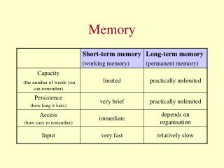
Random Access Memory • Random Access Memory (RAM), a.k.a. main memory is the temporary holding place for code that is being executed, has recently been executed or is soon to be executed, as well as the associated data. • It must be easy and fast to change (write to) in order to work efficiently with the processor.
RAM versus ROM • RAM is distinct from ROM in that it is easily both read and written, whereas, ROM (Read-Only Memory) is easy to read but difficult to write (burn). • RAM is sometimes called Read-Write Memory • RAM also differs from ROM in that RAM is volatile, meaning that it requires power. When the power is turned off, the information is lost.
Blurring the Distinction • NVRAM: Non-Volatile Random Access Memory, is RAM that does not lose its data when the power goes off. • A separate power source such as a battery allows the RAM to hold onto its information until it can be written to more permanent form: to EEPROM or to storage (disk) • Some modems use it to keep phone numbers and/or modem profiles.
Blurring the Distinction II • Flash memory: A version of EEPROM that can be erased and reprogrammed in blocks rather than one byte at a time. This makes writing (burning) easier/faster. • Many PCs use flash memory for their BIOS – a flash BIOS. • Flash memory is often used in modems, as it allows the manufacturer to support new protocols as they become standardized.
Types of RAM • RAM is divided into two main categories: • Static RAM (SRAM) • The value corresponds to a steady current. • Dynamic RAM (DRAM) • The value corresponds to a charge. • It’s “dynamic” because it is hard to keep a charge in a given place. Charges leak away. • When your purpose is to hold a value, being “dynamic” is not good. • The charge has to be refreshed.
SRAM Pros • Speed • SRAM is faster than DRAM, because DRAM requires refreshing which takes time • Simplicity • SRAM is simpler to use than DRAM, again because DRAM requires refreshing
SRAM Cons • Size • SRAM is a more complicated circuit, it involves more transistors than DRAM, and hence it is larger • Cost • Again SRAM is more transistors and so it costs more • Power • Since SRAM involves a constant current, it uses more power than DRAM • Heat • Again since SRAM involves a constant current, it produces more heat
Use of SRAM • Because of the size/cost/power/heat issues SRAM is used sparingly – only when its speed advantage outweighs its many disadvantages. • SRAM is used for cache, which is used to speed up the processor’s interaction with memory.
Main Memory • Because of the size and cost issues, main memory is made of DRAM. • The read action serves to refresh the charge in DRAM. Therefore the refresh cycle effectively consists of reading the memory (though not doing anything with what is read).
Random versus Sequential Access • Memory is written and read in bytes. • The term “random access” implies that a given byte can be accessed (read or written) without proceeding through all of the previous bytes of data being held (as is the case in a sequential devices such as a tape). • A byte is accessed by using its address.
SAM? • What would me mean by SAM?
Bus Keyboard encoder Input port 1 Accumulator Flags ALU Input port 2 Prog. counter TMP Mem.Add.Reg. B Memory C MDR Output port 3 Display Instr. Reg. Output port 4 Control
Memory Address Register • Recall that the Memory Address Register is for holding the address of the memory that is currently being processed. • That memory location may hold an instruction or data (stored program concept). • At this lowest level, addresses are absolute but at a higher level addresses may be relative or absolute.
Question • When the memory address register (MAR) was 32 bits long, we were limited to addressing ____________________ memory locations.
Northbridge middleman • In more sophisticated architectures than the one just considered, the addresses will be placed on the address bus connecting the microprocessor to the Northbridge (or its replacement). • Thus there are two speeds to consider • The bus speeds (address and data) between the processor and Northbridge. • The memory speed between the Northbridge and memory. • Taking advantage of higher FSB speeds requires using faster memory.
Like an Array Two hexadecimal digits shown as the values because we store in byte units.
Two selects • A unit of memory (a cell) has two select inputs (a.k.a. strobes). • The address is split into two parts which can be thought of as the row and the column addresses. • This two-dimensional approach saves on the number of inputs a given memory chip must have. • As the transistor density continues to grow, one of the most difficult aspects of chip engineering becomes having enough external inputs to properly control all of that internal circuitry.
Memory Access and Access Time • Accessing memory, reading or writing it, requires the selection of the appropriate cell. This is handled by the memory controller. • Once a cell has been selected, then information is sent out to the data bus (read) or brought in from the data bus (write). • The time required for select preparation and then the actual reading or writing is known as access time. • Access time is not the only time associated with DRAM. Recall it must also be refreshed periodically.
The steps of a simple read • Place the address on the address bus. • The memory address controller splits the address into two parts. • The lower half (think of it as the row) is sent to the chips. • Once the address has had time to stabilize, a signal is sent telling the memory chips to look at the row address. • A row is now selected. This refreshes the row. (Refreshing is done row by row).
The steps of a simple read (Cont.) • The upper part of the address (the column) is now sent to the chips. • Once the address has had time to stabilize, a signal is sent telling the memory chips to look at the column address. • The data goes from selected cell to buffer (Memory Data Register). • Data goes from buffer to the bus where it is read by processor or whatever.
CAS Latency • CAS: Column Address Strobe Latency • Memory is laid out in rows and columns. • The row address is readied, then there is some delay (known as RAS-to-CAS Delay). Next the column address is readied, then there is a delay and finally one can read or write. This second waiting is known as CAS Latency. • For CAS-2 the wait is 2 clock cycles and for CAS-3 the wait is 3 clock cycles. • But you need a chipset that can take advantage.
Bus Keyboard encoder Input port 1 Accumulator Flags ALU Input port 2 Prog. counter TMP Mem.Add.Reg. B Memory C MDR Output port 3 Display Instr. Reg. Output port 4 Control
Access Time • The time to prepare the address and then read or write the data is known as memory’s access time. • DRAM access times typically fall in the 10’s to 100’s of nanoseconds range. • A nanosecond (ns) is 10-9 s. In a 1-GHz processor, a clock cycle is 1 ns. If DRAM has an access time of 60 ns, this corresponds to 60 of the processor’s clock cycles. • Even this is somewhat misleading since two consecutive accesses to the same memory location may be even slower.
Memory Speed • The speed differences in various DRAM technologies is not so much in different access timesbut in how much data is accessed in an access time. • In addition, since much of the access time involves address preparation. Time can be saved when the next location to be accessed is nearby the one just accessed. • Some DRAM technologies manage to cut down the number of steps involved in subsequent memory accesses.
Speed Comparison • SRAM may typically have an access time of 10 ns compared to DRAM’s 60 ns. Plus SRAM does not have the back-to-back read/refresh issues of DRAM. • On the other hand, disk access speeds fall into the millisecond range, which is hundreds to thousands of times slower than DRAM.
Another Speed Issue • Recall that code that rarely changes, such as the BIOS, is stored in ROM. • Accessing ROM can be slow, with access times in the hundreds of ns, compared to a typical DRAM access time of 60 ns. • To improve access time, the contents of some of the ROM is copied into RAM. This is known as ROM Shadowing. • A device’s Memory Range are memory locations associated with that device to hold its shadowed BIOS. They are placed in what is called “upper memory.” • (Strictly speaking not a system resource.)
Absolute and Relative Address • Data is accessed using its address, there are two ways to address a value • In absolute addressing, the addresses used are the actual addresses of the data (or code) in main memory. • In relative addressing, one does not use the actual address of the data but rather one indicates the offset, i.e. how far the address is from some base address.
Like an Array • Relative Addressing is like an array. • If one refers to the array itself, one is referring to the base address. • The indices then act like the offset, referring one to so many addresses beyond the base. • This is why indices usually start at 0. The first element in the array is stored at the base address, i.e. the offset is 0.
Higher levels • The relative addressing approach is important for any code higher than machine language. • It is not known ahead of time where in memory such code will be loaded and so the relative address approach is required.
Big programs • Relative addressing also allows one to execute a program that is larger than the amount of memory allotted to it. • A large program will be stored on disk, only a portion of it (a page or segment) will be in memory when the program is executing. • When the processor is ready to move onto a different portion of the program, the current page is swapped with a page that is stored on disk.
Paging • The program on disk is laid out using relative addressing. • Then as a section of code is placed in memory (a process known as swapping or paging) the relative addresses are translated into absolute addresses. • During the course of running the program different relative addresses may correspond to the same absolute (physical) address – at different times, of course.
Paging and Non-Paging • At any one time, the memory will have the operating system and various applications in memory. • Applications and some parts of the operating system are swapped in and out. • Other items such as the kernel of the operating system are always in memory. • Thus the memory pool is divided into the paged pool and the non-paged pool.
Virtual Memory • The use of some disk space as an “extension” of memory is known as virtual memory. • Physical memory, on the other hand, is the actual DRAM chips. • The total amount of memory addresses (virtual included) is called the address space.
The Memory Address Bus • There are actually two buses associated with connecting the processor and memory: one for addresses and one for data. • While most specs one hears about concern the memory data bus (the Front-side bus FSB), the address bus is important, especially its width, for determining how many things can be addressed.
Amount of Memory • Because swapping involves accessing the hard disk which is hundreds to thousands of times slower than accessing memory, one wants to limit swapping by having a lot of memory and thus larger pages that require less frequent swapping. • In many cases upping the amount of memory has a more noticeable effect on performance than improving a change in the processor speed.