Download
1 / 45
450 likes | 471 Views
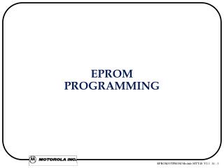
FPGA Based E/EPROM Programmer. By: Jeremy Cooke With Advisor: Dr. Izadi. Presentation Overview. Definitions Project Goals Technologies Used Hardware Design Software Design Problems and Solutions Conclusions. Definitions. E/EPROM Programmer

E N D
FPGA Based E/EPROM Programmer By: Jeremy Cooke With Advisor: Dr. Izadi
Presentation Overview • Definitions • Project Goals • Technologies Used • Hardware Design • Software Design • Problems and Solutions • Conclusions
Definitions • E/EPROM Programmer • A device that can read and write the contents of a variety of non-volatile memory chips • FPGA • Field Programmable Gate Array, a programmable logic device
Project Goals • Design and develop an E/EPROM programmer • Explore advanced digital logic techniques • Learn modern FPGA design techniques • Mix analog and digital circuitry • Interface hardware with Windows based software • Parallel port interfacing techniques • Communications protocol development and implementation
Technologies Used • Field Programmable Gate Array • Digital core • Analog Circuitry • Power Subsystem • Windows Based Software • Programming in Visual C++ 6.0
Hardware Design • Hardware broken into separate analog and digital sections • Digital hardware • Based around an FPGA core • Handles control and coordination of all other components • Controlled by Personal Computer over parallel port • Analog Hardware (Internal Power Supply) • Used for voltage regulation and control • Based around DC-DC converter and adjustable voltage regulators • Controlled by FPGA
Personal Computer FPGA Core Power Supply Memory Device Switching System Hardware Block Diagram Windows Application Software Volatile Circuit
Xilinx FPGA • Excellent for complex digital systems • PROM required for non-volatile operation XC4010XL Field Programmable Gate Array Logic Cells 950 System Gates 7-20K Max RAM Bits 12,800
XC4000 Architecture Programmable Interconnect I/O Blocks (IOBs) Configurable Logic Blocks (CLBs)
C2 C1 C3 C4 H1 DIN S/R EC S/R Control G4 DIN SD G G3 F' YQ Q D Func. G' G2 H' Gen. G1 EC RD 1 H G' Y Func. H' S/R Gen. Control F4 F F3 DIN SD Func. F' XQ F2 Q D Gen. G' F1 H' EC RD 1 H' X F' K XC4000 Configurable Logic Blocks • 2 Four-input function generators • Look Up Tables • 2 Registers • Each can be configured as Flip Flop or Latch
Combinatorial Logic A B C D Z 0 0 0 0 0 0 0 0 1 0 0 0 1 0 0 0 0 1 1 1 0 1 0 0 1 0 1 0 1 1 . . . 1 1 0 0 0 1 1 0 1 0 1 1 1 0 0 1 1 1 1 1 A B Z C D Look Up Tables • Combinatorial Logic is stored in 16x1 SRAM Look Up Tables (LUTs) in a CLB • Example: Look Up Table 4-bit address 4 (2 ) 2 = 64K ! • Capacity is limited by number of inputs, not complexity
XC4000 I/O Block Diagram Vcc Slew Passive Rate Pull-Up, Control Pull-Down T/OE O D Q Output Pad Buffer OK (Output Clock) I 1 Input I Buffer 2 Q D Delay CE IK (Input Clock)
CLB CLB Switch Matrix Switch Matrix CLB CLB Xilinx FPGA Routing • Fast Direct Interconnect – CLB to CLB • General Purpose Interconnect – Uses switch matrix
Programmable Interconnect Points, PIPs (White) Routed Wires (Blue) What's in the chip? Switch Matrix Direct Interconnect (Green) CLB (Red) Long Lines (Purple)
PC FPGA Power Memory Switching How did I use the FPGA? • Used to implement my core digital logic design • As opposed to manually wiring discrete components • Use made design more modular and easy to understand
FPGA External Connections FPGA Memory Data Lines Parallel Port Address Lines Control Lines Voltage Lines
E/EPROM Considerations • For most EPROM types there are corresponding EEPROMs of the same size, density, and compatible chip configuration • Allows for easier support for both technologies
E/EPROM Considerations • EPROM • Usually require 2 voltage levels : Vcc and Vpp • Vpp usually 12 volts or higher • Special erasing procedures • UV Light for example • EEPROM • Usually require only 1 voltage level : Vcc • Erase/Write procedure often as simple as a static RAM device
Vpp Out 5V In 28V Control Lines Vcc Out Control Lines DC-DC Converter 5V to 28V Vpp Level Selector Vcc Level Selector Digital Level Shifting Power Supply
Chip Type Size Vcc (v) Vpp (v) 2716 EPROM 2k*8 5 25 2764 EPROM 8k*8 6 21 27128 EPROM 16k*8 6 21/12.5 27256 EPROM 32k*8 6 12.5 27512 EPROM 64k*8 6 12.5 2816 EEPROM 2k*8 5 NA 2864 EEPROM 8k*8 5 NA 28256 EEPROM 32k*8 5 NA 28512 EEPROM 64k*8 5 NA 28010 EEPROM 128k*8 5 NA 28040 EEPROM 512k*8 5 NA Memory Device Voltage Requirements
Simple 2 Resistor Configuration: R1 = R*(Vout/Vref-1) * In my design R is the parallel combination of resistors Power Supply Calculations
ZIF Socket – Connection to Memory • Zero Insertion Force Socket for memory device to be accessed • Pinout designed to accommodate large variety of chip types • Most pins connected directly to FPGA • Special pins connected to switch interface
Switch Interface For Special Pins • 7 Pins in ZIF socket must be handled specially • They can be a specific analog signal or a specific digital signal depending on the memory device • DIP switches used rather than automated circuitry to reduce complexity
Software Design • Software was created using Visual C++ • Program structure in terms of objects, not just C under C++ • This development environment allowed me to create: • software in an object oriented manner • an easy to use user interface • a professional looking final product in minimal time
Software Design • Bottom up design process • Encapsulate hardware interface routines • lowest level • Create software API • Middle level of abstraction • Create Application Software • Top level
Software Design • This design process enabled me to test and debug the hardware on its lowest level first. • Then I built upon working routines while creating the application software. • Hardware interfacing was less of a concern at this point because all routines have already been created and debugged.
Software Design – Objects • ChipProg Object – Low Level • Initialize/maintain communication with hardware • Configure hardware for specific memory devices • Set/Clear IDB • Send and receive data • Send address and control signal information • Set all voltage levels • ChipAPI Object – Software API • Inherits functionality from ChipProg • Read Byte(s) from specific addresses and ranges • Write Byte(s) to specific addresses and ranges
ChipAPI Object Read Bytes individually or in blocks from specific memory locations Write Bytes individually or in blocks from specific memory locations Application Software Design – Objects ChipProg Object Initialize Hardware Modify Internal Data Bus (FPGA) Set Vpp and Vcc to specific levels Turn Vpp and Vcc on and off Set Address Information Set/Get Data Information Set Control Lines
Software Design – Hardware Testing • Using the ChipProg object as interface to the hardware, I created a simple application to test features of the hardware: • Then I wrote the final application software after all of the basic hardware functions seemed to work properly under software control
Application Software • Memory chip reading and writing utility • Read data into an internal buffer from: • Memory device • Or binary file • Write to memory
Application Software • First a user must select the appropriate memory device • Then reading and writing options are enabled • There are currently 2 memory types supported: • Microchip 28C64A • Generic 27128 Dialog box indicates technical information
The write memory function writes what is currently in the internal buffer to the memory device. • The read memory function allows the user to read a specific address range from the memory device • After reading is complete, the information is stored in an internal buffer, displayed in ASCII and hexadecimal, and the user may save it as a binary file Application Software
Application Software • The memory buffer can be exported or imported to and from a memory file • The current format is raw binary • I plan to support the Motorola S-Record format in the future • Simple buffer operations supported • Fill with value • Clear
Problems • Insufficient pins on FPGA for all functions • Forced manual solution for switching section • Interference from FPGA evaluation board • Timing to ms resolution difficult on PC • Hard to coordinate control signal timing correctly • Control related feedback not available • Sometimes results in errors during block writes
Possible Improvements • Use FPGA without evaluation board and more pins • Design FPGA logic solely with VHDL • Abandon limiting idea to use discrete logic chips • Utilize a microcontroller • Accurate timing • Better communication with PC • USB • More information • Intelligent device • Remove DIP switches and use automated analog switching solution • Analog MUX
Possible Improvements PC mC Power FPGA Memory Switching
Conclusions • This project utilized advanced digital logic techniques • Design and debug of FPGA based systems • Current industry practice • Implementation of a mixed voltage level system • Common requirement in transition to low power systems • As well as a mixed analog/digital system
Idea System Conclusions • Design process for the hardware was a top-down approach • Began with vague requirements and an idea of an end product • Gradually broke ideas down into manageable components • Implemented/debugged each component separately • Combined to create the final hardware system
Hardware Driver Routines System Requirements For Control Conclusions Application • Design process for the software was a bottom-up approach • Hardware already developed so I knew what routines it required for control • Wrote those, encapsulating hardware with a low-level object • Wrote a higher level software object wrapper hiding all low- level hardware interfacing details from application level software • Wrote hardware testing software as well as general application software based on hardware interface routines
Special Thanks • Dr. Izadi - Senior Project Advisor • Information and help regarding all aspects of FPGA based system design • General hardware/software design advice • Continued support through all phases of my project • Professor Otis • Support and advice on microprocessor and microcontroller based system design and interfacing details • As well as gave general advice throughout the life of my project