Download
1 / 30
310 likes | 528 Views
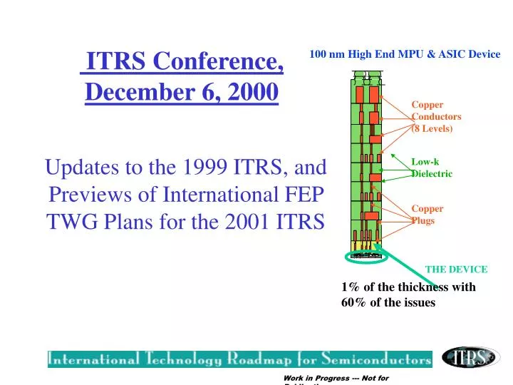
Copper Conductors (8 Levels). Low-k Dielectric. Copper Plugs. THE DEVICE. 100 nm High End MPU & ASIC Device. ITRS Conference, December 6, 2000. Updates to the 1999 ITRS, and Previews of International FEP TWG Plans for the 2001 ITRS. 1% of the thickness with 60% of the issues.

E N D
Copper Conductors (8 Levels) Low-k Dielectric Copper Plugs THE DEVICE 100 nm High End MPU & ASIC Device ITRS Conference, December 6, 2000 Updates to the 1999 ITRS, and Previews of International FEP TWG Plans for the 2001 ITRS 1% of the thickness with 60% of the issues
Covers starting silicon wafer through contact formation and pre-metal dielectric layer deposition Focus has been on requirements for high performance logic transistors & DRAM storage capacitors Mission is to define comprehensive needs and potential solutions for the key technology areas in the front-end-of-line (FEOL) wafer fabrication processing of integrated circuits Scope of FEP TWG Activities
FEP Roadmap Scope A: Gate Stack B: Source/Drain - Extension C: Isolation D: Channel E: Wells F: DRAM Capacitor Stack/Trench G: Starting Material H: Contacts I: PMD
Starting Materials- Tables 32a&b, Figure 17 Surface Preparation-Tables 33a&b, Figure 18 Front End Etch Processes-Tables 34a&B, Figure 21 Transistor Doping-Tables 34a &b, Figure 20 Thermal Processing and Thin Films-Tables 34a &b, Figure 19 Stack Capacitor- Table 35, Figure 22 Trench Capacitor-Table 36 Device Modeling Thrusts & Sub-TWG Organization
Overall & Table 31: Mike Jackson- Mike.Jackson@sematech.org Walter Class- Walter.Class@axcelis.com Tables 32a & 32b: Howard Huff- howard.huff@sematech.org David Myers- d-myers@ti.com Tables 33a & 33b: Scott Becker- sbecker@fsi-intl.com Glenn Gale- GGale@aus.telusa.com Tables 34a &b Etch: Robert Kraft- r-kraft2@ti.com Tables 34a &b Doping: Larry Larson- larry.larson@sematech.org Kevin Jones- kjones@eng.ufl.edu Tables 34a&b Carlton Osburn- osburn@eos.ncsu.edu Thermal/Films: Howard Huff- howard.huff@sematech.org Contacts for Commentary & Criticism
Table 35: Seiichiro Kawamura - RHD01125@nifty.ne.jp Table 36: Martin Gutsche - Martin.Gutsche@infineon.com Contacts for Commentary & Criticism
Copper Conductors (8 Levels) Low-k Dielectric Copper Plugs THE DEVICE 100 nm High End MPU & ASIC Device 2000 Update- Overview of changes 1% of the thickness with 60% of the issues
Since publication of the 1999 ITRS device scaling has occurred more rapidly than forecasted Several manufacturers are forecasting 130nm node device manufacture in the year 2001, rather than 2002 as originally forecasted The MPU/ASIC technology gap has been eliminated Leading edge MPU and ASIC gate lengths are now equal Recognition of widespread industry practices that yield a physical gate lengths that are smaller than the resist printed feature size The DRAM Stack capacitor scaling (cell “a” Factor) is scaling more slowly than forecasted. DRAM storage cell areas shrink less rapidly than 1999 forecast 450mm wafers may be required earlier than originally forecasted Summary of Major Changes since 1999
Starting Materials & Surface Preparation Update & 2001 Plans Technical Requirments Tables 32a&b and Tables 33a&b
1999 ITRS Tables 32a & b, and Tables33a&b have not been updated to reflect the new proposed technology node parameters Changes have a very significant effect on bulk and surface defect requirements Defect requirements also have a very strong impact on wafer cost and availability New tables will be generated when technology node consensus is achieved, and new, validated yield/defect algorithms have been generated Summary of Actions and Plans for Starting Materials & Surface Preparation
Node Changes Drive New Defect Requirements for Starting Materials and Surface Preparation New DRAM cell “a”factors and Bit Capacity New Starting Materials Metal,COPS, Particle, & SF Requirements New Lithography Field Sizes New Chip Sizes, “Active Areas”, &Kill Ratios Statistics Based Defect-yield Algorithm New MPU Cache Requirements New Surface Prep Particle, Metal, and Water Mark Requirements New MPU & DRAM 1/2 pitch and gate lengths Cost Considerations
Update and Validate inputs to the the Defect-Yield Algorithms used to generate defect requirements forecasts Reverse engineering studies of current manufactured products to validate Chip Size DRAM, SRAM and Logic transistor densities DRAM, SRAM, and Logic active areas Develop methodology for forecasting chip size, transistor densities and active areas Apply Statistical Yield/Defect equation to new validated parameters to re-forecast future defect requirements. Begin discussion on 450mm wafer requirements. Starting Materials and Surface Preparation 2001 Plans
Thermal Thin Films, Gate Etch, and Doping Updates and 2001 Plans RequirementsTables 34a & b Potential Solutions Figures 19, 20, & 21
Tables 34a &b 2000 updated for years 1999, 2000, & 2001 to reflect current transistor gate lengths in production. Remaining updates will be made in 2001 upon achievement of consensus regarding new forecasts for ASIC and MPU gate lengths New forecasted physical gate lengths will have the effect of bringing “red walls” closer. 2004 need for high k gate dielectric materials 2004 need for dual metal gates 2004 need for ultra-shallow highly activated drain extensions Summary of actions and plans
Thermal Films Year 2001Issues • Accelerated MOSFET gate length scaling creates: • Accelerated need for high-k gate dielectric solution • Accelerated need for dealing with increased MOSFET leakage • Concurrent ASIC and MPU accelerated solutions • The achievement of the high-k dual metal gate solution is • unlikely in the 2004 time frame
Transistor Contact & Doping- 2001 Issues • Accelerated MOSFET Gate Length Scaling Creates: • Accelerated need for dual metal gate electrodes • Accelerated need for next generation contact solutions • Accelerated need for ultra-shallow highly activated extensions • ASIC and MPU accelerated solutions that are concurrent in time • Achievement of these solutions by 2004 is questionable
Scaled MOSFET’s with Ion/Ioff tailored for specific applications High performance desktop Low Operating Power Low Standby Power Embedded DRAM transfer devices Multiple Tailored MOSFET’s on the same chip Doping strategies to achieve dynamic threshold voltage adjustment Design approaches for power management Expanded use of SOI for low power applications Potential Interim Scaling Solutions
Forecast scaling-driven MOSFET technical requirements and potential solutions for: Desktop applications Low operating power applications Low standby power applications embedded DRAM transfer devices Expand roadmap scope by developing new requirements for pre-metal dielectric layers Logic devices DRAM’s 2001 ITRS Plans for Thermal Films & Doping
Proposed New Physical Gate Length Issues • 1999 ITRS assumed post-etch gate length equal to feature size printed in the resist • Industry practice has been to vary the gate etch process to achieve a physical gate length • after etch that is smaller than the printed feature size • New proposed reduced post-etch gate length is achieved more complex etching processes • New etch processes add variance to the final physical gate length • Two etch processes have been identified that result in a reduced post-etch gate length
Gate Etch Proposed Process Alternatives Resist Polysilicon Gate Material Silicon Resist Isotropic Etch Poly Vertical Etch Poly Isotropic Etch Poly Vertical Etch
Collaborate with Lithography TWG to develop a variance budget for Lithography and CD Etch Proposed budget; Lithography = 2/3 of total allowed variance CD Etch = 1/3 of total allowed variance Generate new CD Etch requirements needed to conform to allowed variance budget Year 2001 CD Etch Process Plans
Impact of New DRAM cell “a” Factor Stack Capacitor Height, Shape, Electrode Material, Dielectric value & Layer Thickness FEP Table 35 Cell Area Factor “a” Chip Area Available for 35fF Storage Capacitor Cell size = aF2 Trench Depth, Trench Capacitor Shape, Electrode Material, Dielectric value & Layer Thickness DRAM 1/2 Pitch, “F” FEP Table 36
DRAM Cell size factor and Cell size 10 1 8 0.1 6 Cell size (um2) Cell size factor a 4 0.01 ITRS ‘99 ITRS ‘99 2 ITRS 2000 ITRS 2000 0 0.001 35 180 100 130 70 50 35 180 100 130 70 50 Technology Node (nm) Technology Node (nm)
DRAM Capacity and Die size 1000 1000 ITRS ‘99 ITRS 2000 800 100 600 X4/4Years DRAM Capacity (G bit) Chip size (mm2) 400 X4/5Years 10 ITRS ‘99 200 ITRS 2000 X4/4Years 1 0 35 180 100 130 70 50 35 180 100 130 70 50 Technology Node (nm) Technology Node (nm)
Calculated DRAM chip size 128G 16G 32G 64G 8G 4G 2G Introduction 1chip/Field 1G Production 2chips/Field 4G 8G 16G 2G 32G 1G 512M 256M Year
Increased cell “a” factor (2000 update) results in larger chip area allocation for storage cell chip size for a given DRAM capacity is increased Storage capacitor scaling requirements less challenging Proposed, more aggressive, DRAM 1/2 Pitch scaling (2001 ITRS) results in smaller chip area allocation for storage cell chip size for given DRAM capacity is decreased Storage capacitor scaling requirements become more challenging Summary of year 2000 & 2001 DRAM Issues
2000 Update: Tables 35 & 36 Updated to reflect new DRAM cell area factors Less aggressive “a” factors increase storage area size Impacts future chip sizes and future bits/Chip Tables 35 & 36 not updated to reflect new proposed 2001 DRAM 1/2 pitch forecasts Year 2001 Plans Update Tables 35 & 36 to reflect consensus DRAM 1/2 pitch forecasts Continue to review DRAM chip size, “a” factor and future bits/chip Year 2001 New Memory Projects Generate New Requirements for Flash Memory (Europe TWG) Generate New Requirements for Ferroelectric RAM (Japan TWG) Memory Year 2000 Update and 2001 Plans


![2008 ITRS Emerging Research Materials [ERM] December 6, 2008](https://cdn2.slideserve.com/4220113/2008-itrs-emerging-research-materials-erm-december-6-2008-dt.jpg)