Download
1 / 3
30 likes | 208 Views
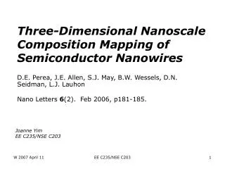
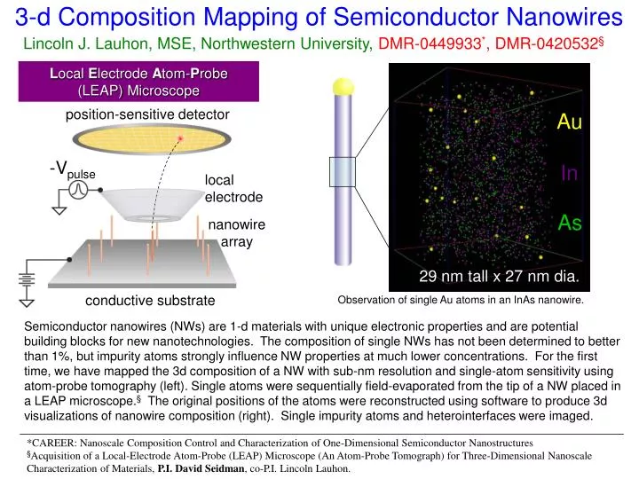
3-d Composition Mapping of Semiconductor Nanowires. -V pulse. Au. In. As. conductive substrate. 29 nm tall x 27 nm dia. Lincoln J. Lauhon, MSE, Northwestern University, DMR-0449933 * , DMR-0420532 §. L ocal E lectrode A tom- P robe (LEAP) Microscope. position-sensitive detector.

E N D
3-d Composition Mapping of Semiconductor Nanowires -Vpulse Au In As conductive substrate 29 nm tall x 27 nm dia. Lincoln J. Lauhon, MSE, Northwestern University,DMR-0449933*, DMR-0420532§ Local Electrode Atom-Probe (LEAP) Microscope position-sensitive detector local electrode nanowire array Observation of single Au atoms in an InAs nanowire. Semiconductor nanowires (NWs) are 1-d materials with unique electronic properties and are potential building blocks for new nanotechnologies. The composition of single NWs has not been determined to better than 1%, but impurity atoms strongly influence NW properties at much lower concentrations. For the first time, we have mapped the 3d composition of a NW with sub-nm resolution and single-atom sensitivity using atom-probe tomography (left). Single atoms were sequentially field-evaporated from the tip of a NW placed in a LEAP microscope.§ The original positions of the atoms were reconstructed using software to produce 3d visualizations of nanowire composition (right). Single impurity atoms and heterointerfaces were imaged. *CAREER: Nanoscale Composition Control and Characterization of One-Dimensional Semiconductor Nanostructures §Acquisition of a Local-Electrode Atom-Probe (LEAP) Microscope (An Atom-Probe Tomograph) for Three-Dimensional Nanoscale Characterization of Materials, P.I. David Seidman, co-P.I. Lincoln Lauhon.
3-d Composition Mapping of Semiconductor Nanowires Catalyst-nanowire interface 23x14x14 nm3 23x14x14 nm3 Au In As 29 nm tall x 27 nm dia. 10 nm dia X 1 nm thick slices Lincoln J. Lauhon, MSE, Northwestern University,DMR-0449933, DMR-0420532 The positions of single gold atoms within an InAs nanowire are visualized below. Only 2% of In and As atoms are shown to highlight the gold. The gold atoms are trapped in the nanowire during the growth, which is directed by a liquid gold catalyst (at right). Perea et al, submitted to Nano Letters.
3-d Composition Mapping of Semiconductor Nanowires Lincoln J. Lauhon,MSE, Northwestern University,DMR-0449933*, DMR-0420532§ Outreach Education & Training Prof. Lauhon is the faculty director of the Research Experience for Science Teachers (REST) program at Northwestern. He recently gave a presentation on nanoscale composition mapping to REST participants as part of a professional development workshop organized by the Nanoscale Science and Engineering Center for Learning and Teaching (NCLT). A video of the presentation will be available on the NCLT website http://www.nclt.us/ pending publication of the research results. Daniel Perea, a first year grad student of Mexican descent, performed the atom-probe research shown here and has submitted a manuscript to Nano Letters. In October, he will present his work at the annual conference of the Society for the Advancement of Chicanos and Native Americans in Science (SACNAS). Danny was one of two students selected to represent Northwestern University at this conference. Danny Perea *CAREER: Nanoscale Composition Control and Characterization of One-Dimensional Semiconductor Nanostructures §Acquisition of a Local-Electrode Atom-Probe (LEAP) Microscope (An Atom-Probe Tomograph) for Three-Dimensional Nanoscale Characterization of Materials, P.I. David Seidman, co-P.I. Lincoln Lauhon.