Download
1 / 20
210 likes | 408 Views
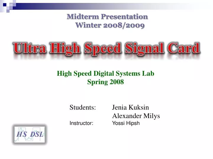
Midterm Presentation Winter 2008/2009. Ultra High Speed Signal Card. High Speed Digital Systems Lab Spring 2008 Students: Jenia Kuksin Alexander Milys Instructor: Yossi Hipsh. Goal of Our Meeting. Design Review of project schematics before proceeding to PCB design.

E N D
Midterm Presentation Winter 2008/2009 Ultra High Speed Signal Card High Speed Digital Systems Lab Spring 2008 Students: Jenia Kuksin Alexander Milys Instructor: Yossi Hipsh
Goal of Our Meeting • Design Review of project schematics before proceeding to PCB design. • Receiving feedbacks and general notes.
Project Description • Designing High Speed Transmission Line Board which will provide an ideal vehicle for learning about Signal Integrity issues like: • Reflections in Transmission Lines • Cross Talk in Transmission Lines • Jitter • Skew
Experiment Environment Instructor High Speed Transmission Line Board Controller Switching System Pulser Transmission Lines Array Student
Block Diagram Controller S1 Will be OE for splitters S3 Connects One channel from 36 To scope S2 Connects One channel from 36 To scope S0 0narrow pulse 1wide pulse Analog Switches Analog Switches Pulser Signal Splitter Z(Source) Transmission Lines 36 lines Termination Z(Load) 1 36 36 36 S5 Control for MCP195 (jitter)
Description of Main Blocks • Pulser - will create short (0.5-1 nsec) and a long (10-13 nsec) pulse signal with very low rise/fall time (200ps) . (will be implemented by Yossi’sGroup) • Signal Splitter – launching a signal into a transmission line and converts differential signal to single ended while only one line can be alive at the same time • Analog Switches – transmit the measured voltage signal on input/output of selected transmission line to oscilloscope.
Description of Blocks • Transmission Lines – will contain 36 microstrip, single ended transmission lines with different terminations. • Controller – Controls all of the operation of the Board. (will be implemented by Mony’s Group)
Pulser-Block Diagram Translator MC100EPT20 3.3V ECL Programmable Delay Chip Splitter MPC94551 MC100EP195 3.3V / 5V ECL 2-Input Differential AND/NAND One Shot MC74LCX74DG Oscillator 50MHz C01025 11 MC100EP05 CMOS 5V/3.3V CMOS 3.3V Translator MC100EPT20 3.3V ECL Programmable Delay Chip MC100EP195 11 Controller 3
One Shot Simulation in Hyperlynx Pulse width from one-shot is determined by capacitor and resistor Twidth=9.37ns R=100 ohm C=130 pF
Signal Splitter Block Diagram Differential lines Single ended lines Single ended lines From Pulser To Transmission lines Single ended Termination Differential Termination 36 Amplifiers 36 36 1:10 Differential Clock Driver MC100LVEP111FAG 1:10 Differential Clock Driver MC100LVEP111FAG 10 6 1:10 Differential Clock Driver MC100LVEP111FAG 10 Voltage Regulator 1:10 Differential Clock Driver MC100LVEP111FAG 10 Controller
A B C D A E B F C SP6T Switch D E F SP6T Switch Analog Switches Block Diagram 36 Transmission Lines 36 hot lines 36 hot lines 3 Control lines 3 Control lines 6 hot lines 6 hot lines 3 Control lines 1 hot line 1 hot line 3 Control lines SP6T Switch Ch1 SP6T Switch Ch2
6 Inputs 3Controls SP6T Switch Output Single Switch Diagram We use Block of SP6T Analog Switches to connect Inputs and Outputs of transmission lines to Channels of Digital Oscilloscope. SP6T Switch MASWCC0006 V3
PCB placement (preliminary) Digital part Analog part Main Power Regulation Local LDO Control Analog MUX Analog MUX Control Pulser Digital Splitter Amplifiers + Local LDO Transmission Lines
PCB Stackup(preliminary) Signals(microstrip) FR4 GND FR4 Vt_1v3 – stripline (mux-measurement) FR4 Vcc_3v3 FR4 Signal_control_1 FR4 Vcc_5v (Vcc_5v5) FR4 Signal_control_2
Parts List • Missing parts • SW90-0004A- GaAs SP6T Switch, Absorptive, Single Supply • CD74HCT237 – High Speed CMOS Logic, 3-to-8 Line Decoder Demultiplexer with Address Latches - • GVA-84+ - 5 Volt-Surface Mount Monolithic Amplifer • RFC1 ADCH_80A -
Time Shedule We are at that stage
Current tasks PCB Designing – 3 weeks PCB Production – 3 weeks PCB Assembly – 3 weeks Functional tests – 1 week