Download
1 / 16
190 likes | 314 Views
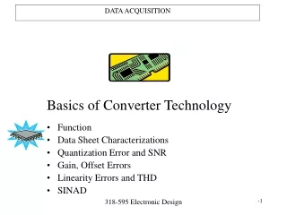
DATA ACQUISITION. Basics of Converter Technology Function Data Sheet Characterizations Quantization Error and SNR Gain, Offset Errors Linearity Errors and THD SINAD. DATA ACQUISITION BASICS. ANALOG VOLTAGE RANGE VFS QUANTIZED INTO 2 n LEVELS WHERE n = # OF BITS.

E N D
DATA ACQUISITION Basics of Converter Technology • Function • Data Sheet Characterizations • Quantization Error and SNR • Gain, Offset Errors • Linearity Errors and THD • SINAD 318-595 Electronic Design
DATA ACQUISITIONBASICS ANALOG VOLTAGE RANGE VFS QUANTIZED INTO 2n LEVELS WHERE n = # OF BITS Nominal Quantization Step 0 1 2 3 4 5 6 7 8 9 10 11 Nominal Step Size Q = VFS/2n Highest Voltage Step = VFS – Q Max Count = 2n–1 (0 is a valid step) 318-595 Electronic Design
Quantization Error Note: Last step occurs at VFS(N-1)/N under ideal conditions Voltage is Measured as Fraction of a reference Vref VFS = Vref Quantization Error Ideal 3 Bit A/D Converter Transfer Function 318-595 Electronic Design
n D/A A/D • Max Quantization Error: • Qerr = VFS/(2n) = 1 bit 318-595 Electronic Design
SNR = 20 log(2(n-1) * sqrt(6) ) = 20log (2(n-1)) + 20log (sqrt(6)) = 20(n-1)log(2) + 20log (sqrt(6)) = 20nlog(2)-20log(2)+20log (sqrt(6)) = 20nlog(2) + 20log (sqrt(6)/2) = 6.02n + 1.76 n D/A A/D Sinewave MAX SNRDB = 6.02n + 1.76 • Max Quantization Error, Qerr = VFS/(2n) = 1 bit • More Resolution (higher n) means less quantization error • Examples: • VFS = 10V, n = 8 Bit, Qerr = 39.96mV, SNRmax = 49.9DB • VFS = 10V, n = 12Bit, Qerr = 2.44mV, SNRmax = 74.0DB • VFS = 10V, n = 16Bit, Qerr = 0.16mV, SNRmax = 98.1DB • More Resolution may require, slower speed, higher power 318-595 Electronic Design
Offset Error • Example of ½ Bit Offset Error • Offset Error: Shifts Ideal Staircase Function Right (+) or Left (-) by Max Voltage or Max LSBs 318-595 Electronic Design
Gain Error • Gain Error will change the converter “slope” • Gain Error: Changes Ideal Staircase Function so that last step is not at VFS(N-1)/N 318-595 Electronic Design
Integral Linearity Error: Max Deviation from Ideal Straight Line (INL: Integral Non-Linearity) Xfer Curve drawn at midpoint of each input step (ideal vs actual) 318-595 Electronic Design
Differential Linearity Error: Max Deviation from Ideal Step Size (DNL: Differential Non-Linearity) DNL max > 1 Bit can lead to missing codes 318-595 Electronic Design
Linearity Errors Induce Harmonic Distortions D/A 318-595 Electronic Design
SINAD: Signal-to-Noise Ratio and Distortion • ENOB: Effective Number of Bits • Combination of SNR and THD specifications • Measure of overall “usable” Dynamic Performance In Ideal Converter ENOB = n 318-595 Electronic Design
Power Supplies are Extremely Important !! • PSRR: Power Supply Rejection Ratio • Measure of output noise injected by PS noise • PSRR is function of frequency • Degrades with frequency • A/D converters require “quiet” supply voltages • Use adequate bypass capacitances • Isolate supply voltages using separate regulators 318-595 Electronic Design
DATA ACQUISITION A/D Converter Architectures • Flash High Speed, High Power • Integrating High Resolution, Parallel • Successive Approximating Low Resolution, High Speed 318-595 Electronic Design
Successive Approximating (SAR) END OF CONV SUCCESSIVE APPROXIMATION REGISTER n-1 n-2 n-3 Decision signal n OUTPUT BITS CONTROL CLOCK Clock n-n V Ref n-1 B BIT D/A Converter COMPARATOR n-2 n-3 V in Buffer n-n 318-595 Electronic Design
Integrating COUNTER n-1 n-2 n Output Bits n-3 V in Buffer n-n CLOCK Clk COMPARATOR Clr Current Source CONTROL I C 318-595 Electronic Design
FLASH V Ref OUTPUT LOGIC REGISTER n-1 n-2 n-1 n Output Bits n-2 V in BUFFER n-3 n-n 2n –1 COMPARATORS 1 318-595 Electronic Design