Download
1 / 20
200 likes | 485 Views
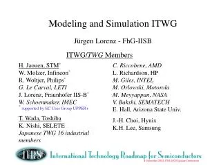
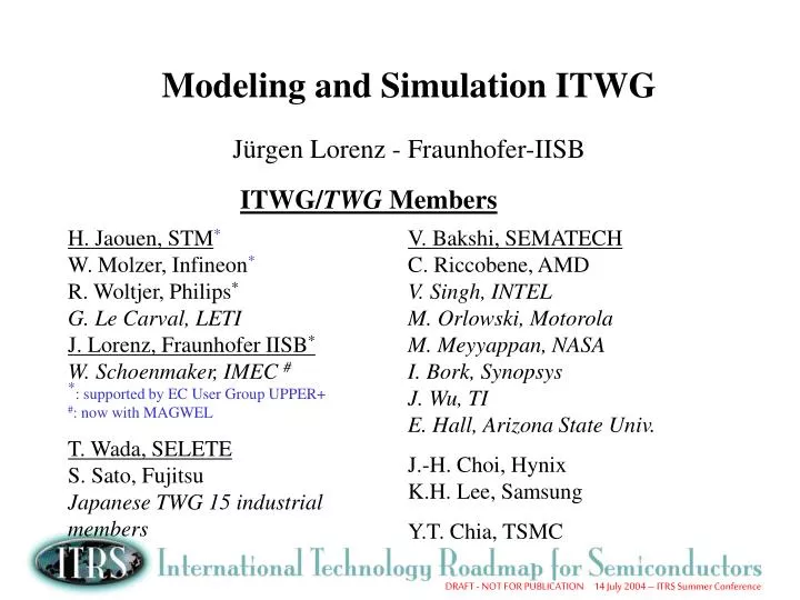
Modeling and Simulation ITWG Jürgen Lorenz - Fraunhofer-IISB. ITWG/ TWG Members. H. Jaouen, STM * W. Molzer, Infineon * R. Woltjer, Philips * G. Le Carval, LETI J. Lorenz, Fraunhofer IISB * W. Schoenmaker, IMEC # * : supported by EC User Group UPPER+ # : now with MAGWEL

E N D
Modeling and Simulation ITWG Jürgen Lorenz - Fraunhofer-IISB ITWG/TWG Members H. Jaouen, STM* W. Molzer, Infineon* R. Woltjer, Philips* G. Le Carval, LETI J. Lorenz, Fraunhofer IISB* W. Schoenmaker, IMEC # *: supported by EC User Group UPPER+ #: now with MAGWEL T. Wada, SELETE S. Sato, Fujitsu Japanese TWG 15 industrial members V. Bakshi, SEMATECH C. Riccobene, AMD V. Singh, INTEL M. Orlowski, Motorola M. Meyyappan, NASA I. Bork, Synopsys J. Wu, TI E. Hall, Arizona State Univ. J.-H. Choi, Hynix K.H. Lee, Samsung Y.T. Chia, TSMC
Technology Modeling SCOPE & SCALES • Equipment related • Equipment/Feature scale Modeling • Lithography Modeling • Feature scale • Front End Process Modeling • Device Modeling • Interconnects and • Integrated Passives Modeling • IC-scale • Circuit ElementsModeling • Package Simulation •Materials Modeling •Numerical Methods
Key Messages (I) • Mission of Modeling and Simulation as cross-cut topic: • Support areas covered by other (especially focus) ITWGs • In-depth analysis of M&S needs of other ITWGs performed, based on • documents + inter-ITWG discussions • Modeling and simulation provides an ‘embodiment of knowledge and understanding’. It is a tool for technology/device development and optimization and also for training/education • Technology modeling and simulation is one of a few enabling methodologies that can accelerate development times and reduce development costs: Assessment up to 35% in 2003 • important not only in years of difficult economic conditions
Key Messages (II) • Art of modeling: • - Combine dedicated experiments & theory to extract physical mechanisms • & parameters • - Find appropriate trade-off between detailed physical simulation (CPU and • memory costly) and simplified but physically appropriate approaches • Accurate experimental characterization is essential • Further growing importance of atomistic/materials/hierarchical/multilevel simulation - appropriate treatment of nanostructures • Need for additional participation esp. from Korea and Taiwan
Crosscuts between M&S and other ITWGs • Detailed analysis of other ITRS chapters + discussions with other ITWGs as basis for 2003 M&S challenges and requirements tables, and text • This process is continued in 2004 - emphasis on tables - also as preparation for 2005 • Crosscuts with focal ITWGs and other cross-cut ITWG described in detail • Links with ALL other ITWGs. Some examples: • Design: Influence of process fluctuations, intrinsic statistics, noise, • reliability, ... on design • Test: Extension of interconnect simulation towards simulation • of test equipment • PIDS: Long list including modeling of new materials and new • device architectures, atomistic/quantum mechanical • simulation, fluctuations and variations, • coupled device/circuit/system simulation
Crosscuts between M&S and other ITWGs (cont.) • Some examples (cont.): • FEP: Long list including modeling of material issues, • new device architectures, ultra-shallow junctions and • defect engineering, assessment of process variants • Lithography: Push limits of optical lithography by optimization of • options; assessment of Next Generation Lithography • based on predictive physical models (e.g. efficient • solution of Maxwell equations) • Interconnects: Large range of M&S support needed, from prediction of • material properties (e.g. resistivitiy of narrow Cu lines) to • impact of non-idealized interconnects on IC layout • Factory Int.: Support shrink of technology implemented in fab line, • by equipment/process/device/circuit simulation. • Assess impact of process variations on yield
Crosscuts between M&S and other ITWGs (cont.) • Some examples (cont.): • Assembly and Packaging: • Co-design issues: Chip and package, • mechanical/electrical/thermal simulation • ESH: Bi-directional link w.r.t characterization and models for • gas composition and chemical reactions • Yield Enhancement: • Simulation influence of defects and of • process fluctuations on devices/ICs/yield • Metrology: M&S needs advanced metrology for development/ • assessment of physical models. • Physical modeling to support metrology e.g. w.r.t. linking • measured spectra to gas composition, interpretation of • measured data, extension of measurements from 2D to 3D
Short-Term Challenges: 2003 and 2004 Changes • 2003 ITRS • Modeling hierarchy included “Modeling of shallow junctions” extended • to “Front-End Process Modeling for Nanometer Structures” • • “Ultimate nano-scale CMOS simulation capability” pulled in from long-term, replacing & partly incorporating “Gate-stack models for ultra-thin dielectrics” (phenomenological models) • • 2002 long-term challenge “Thermal-Mechanical-Electrical Modeling for interconnections and packaging“ pulled in from long-term (6th short-term challenge) • More precise phrasing & shift of emphasis / new aspects in other challenges • 2004 ITRS: • High-frequency Device and Circuit Modeling for • 5–100 GHz Applications • Challenge “Modeling of Equipment Influences on Features Generated in Deposition and Etching Processes“ updated to “Integrated Modeling of Equipment, Materials, Feature Scale Processes and Influences on Devices” • Additionally stress co-design with packaging; reliability
2003 Difficult Challenges > 45 nm Grand Challenge Grand Challenge
2003 Short-term Difficult Challenges High-Frequency Circuit Modeling for 5-40 Ghz Applications • Needs • Efficient extraction and simulation of full-chip interconnect delay • Accurate and yet efficient 3D interconnect models, esp. for transmission lines and S-parameters • High-frequency circuit models including • non-quasi-static effects • substrate noise • parasitic coupling • Parameter extraction assisted by numerical electrical simulation instead of RF measurement • Identified as one of the Grand Challenges ! (From Philips)
2003 Short-Term Difficult Challenges Front-End Process Modeling for Nanometer Structures Needs • Diffusion/activation/damage models and parameters incl. low thermal budget processes in Si-based substrate, e.g. Si, SiGe:C, (incl. strain), SOI and ultra-thin body devices • Characterization tools for ultra-shallow geometries and dopant levels • Modeling hierarchy from atomistic to continuum for dopants and defects in bulk and at interfaces • Identified as one of the Grand Challenges ! Source: A. Claverie, CEMES/CNRS, Toulouse, France
2003 Short-Term Difficult Challenges Modeling of Equipment Influences on Features Generated in Deposition and Etching Processes Needs • Fundamental physical data ( e.g. rate constants, cross sections, surface chemistry); reaction mechanisms and reduced models for complex chemistry • Linked equipment/feature scale models • CMP (full wafer and chip level, pattern dependent effects) • •MOCVD, PECVD and ALD modeling • • Multi-generation equipment/wafer models Simulated across-wafer variation of feature profile for a sputter-deposited barrier. (From Fraunhofer IISB)
2003 Short-Term Difficult Challenges Lithography Simulation including NGL Needs • Optical simulation of resolution enhancement techniques including mask optimization (OPC, PSM) • Predictive resist models incl. line-edge roughness, etch resistance and mechanical stability • Multi-generation lithography system models Printing of defect on phase-shift mask: bump defect (top) vs. etch defect (lower) (From Fraunhofer IISB)
2003 Short-Term Difficult Challenges Ultimate Nanoscale CMOS Simulation Capability Pulled in from long-term in 2003! Needs • Methods and algorithms that contribute to prediction of CMOS limits • Quantum based simulators • Models and analysis to enable design and evaluation of devices and architec- tures beyond traditional planar CMOS • Phenomenological gate stack models for ultra-thin dielectrics • Models for device impact of statistical fluctuations in structures and dopant distributions classical quantum drain source courtesy Infineon / TU Munich courtesy Infineon / TU Munich Quantum-mechanical vs. classical carrier densitiy in double-gate transistor
2003 Short-Term Difficult Challenges Thermal-Mechanical-Electrical Modeling for Interconnections and Packaging Pulled in from long-term in 2003! Needs • Model thermal-mechanical and electronic properties of low-k, high-k and conductors and the impact of processing on these properties • Model reliability of packages and interconnects, e.g. stress voiding, electromigration, piezoelectric effects; textures, fracture, adhesion courtesy TU Vienna / IST project MULSIC Temperature distribution in an interconnect structure
Long-Term Challenges: 2003 Status and 2004 Changes • “Extend beyond continuum tools” in 2003 shifted to short-term & integrated • there into various challenges, esp. “Front-End Process Simulation” • Instead: “Modeling of processing and electrical properties of new materials” - 2004 changed to “Modeling of Chemical, Thermomechanical, and Electrical Properties of New Materials“ - rest of 2002 short-term challenge “Gate-stack models for ultra-thin dielectrics” included here • “Ultimate nanoscale CMOS simulation capability“ in 2003 shifted • to short-term, including parts of old „gate stack modeling“ challenge • “Thermo-Mechanical-Electrical Modeling for Interconnections and Packaging” shifted to short-term in 2003 • “Software Module Integration” skipped: Rather a requirement than a • challenge • Instead in 2003: “Nano-Scale Modeling” (e.g. nanotubes ...) • New 2003 challenge “Optoelectronics modeling”
2003 Difficult Challenges < 45 nm Grand Challenge
Short-Term Requirements: 2003 Status & 2004 Discussion • General: • - Some items now in “zebra” colour - according to ITRS guidelines: • “Limitations of available solutions will not delay the start of production. In some cases, work-arounds will be initially employed. Subsequent improvement is expected to close any gaps for production performance in areas such as process control, yield, and productivity.“ • This means for simulation: It can be used, but with more calibration, larger CPU time/memory, less generality then in the end required ... • Items adapted to 2 years passed since 2001 ITRS & changes in requirements/technical progress • Lithography: • - In exposure simulation no more emphasis on evaluation of wavelengths, but on capabilities of simulation incl. mask features and CPU efficiency • - New: Full-chip lithography simulation
Short-Term Requirements: 2003 Status & 2004 Discussion Gate stack: Short-term focus on high-k Back-End Process/Equipment/Topography Modeling: - More clear structure, according to kinds of processes to be simulated Numerical device modeling: - Instead of “bulk CMOS” and “non-bulk” CMOS now “Classical CMOS” and “Non-classical CMOS incl. channel-engineered devices” - 2004: add “Novel memory devices” and “reliability” “Circuit element modeling/ECAD” replaced by “circuit component modeling”& now structured into “active devices” and “Interconnects and integrated passives”. 2004: add “Process and Materials Impact on Electrical Performance“ Package modelingnow structuring into “electrical modeling” and “thermo-mecha- nical modeling” instead of an item “thermo-mechanical-electrical integrated models”.2004: add “Material Properties”
More details given in tables & ITRS text • Thank you