Download
1 / 23
250 likes | 430 Views
DC/DC Power Supply. By Rob McMurry Jason Wells. Presentation. Objectives Design Layout Design Issues & Problems Results Conclusions. Objectives. Input range of 36 - 48 Volts Outputs of +5,+12,-12 Volts Total power of 50 W (10/20/20) Ripple ± 2. 5%

E N D
DC/DC Power Supply By Rob McMurry Jason Wells
Presentation • Objectives • Design Layout • Design Issues & Problems • Results • Conclusions
Objectives • Input range of 36 - 48 Volts • Outputs of +5,+12,-12 Volts • Total power of 50 W (10/20/20) • Ripple ± 2.5% • Improve Line and Load Regulation through the implementation of feedback control • Use a switching frequency of 70 kHz
Overview of Circuit Operation • Self starting Resistive Bridge • Provides enough voltage to start the first gate drive which then provides voltage for the PWM chips thus eliminating the need for additional external voltages sources or batteries. (adds a loss of approximately 1.5 Watts) • Flyback Converters • Energy is transferred from the input to the output through storage element. This element is the inductor of the circuit. • When switch is on, current flows into the primary side inductor. The switch then turns off and the stored energy is forced to flow in the secondary winding into the output.
Overview of Circuit Operation(cont.) • Flyback Converters (cont.) • Separate switches and sense inductors allows for individual control of each output voltage. • Separate secondary windings provides isolation between the outputs and the input voltages.
Overview of Circuit Operation(cont.) • PWM switching circuits • The UC3844 takes a generates a gate drive pulse which is used to control the FET’s in each of the converters. • Since our control did not function correctly in the circuit, two variable resistors were used to control the frequency and duty ratio. • Snubber • A turn-off snubber was added to each of the FET’s to reduce voltage over shoot and switching losses.
Overview of Circuit Operation(cont.) • Control • -6 V reference voltage was generated by using a op-amp to invert and divide the output of a 12 V regulator. • Input and out put voltages are added in through a summing inverter circuit to give an ultimate output voltage equation of Vo = (Vref - .05Vin - .05Vout)*22,000/Rgain .
Flyback Inductor Size Calculation • L=Vin*dt/di In Flyback Converters, di=load current dt=D/freq. For 12V L=103uH For 5V L=34.28uH These are the minimum values for the inductors for continuous mode (i.e. Iload does not equal zero at any point)
Flyback Inductor Physical Design • Must be above critical inductance • 1 to 1 transformer turns ratio • Must have a core with high permeability that will not saturate • Pot Cores were used (L = .1106 mH / turn) • 3 transformer/inductors were used • 1) and 2) two 10 turn windings and a 25 turn windings were used with resulting inductance of 1.10mH and 2.76mH • 3) had two 10 turn windings giving 1.10mH each and a 60 turn winding giving 3.31 mH
Capacitor Design • For Flyback Converters I=C*dv/dt I=(Pout)/(Vout) dv=Vout*5% dt=D/frequency freq.=70kHz Capacitor values for 12V is C=10uF 5V is C=7.14uF Consequently the capacitor values have to be greater than these values for 5% ripple and below
Wire Gauge Sizing • Windings for the ± 12 V: • Max average current occurs at Pmax, Vmin(in) • (Iave(in) +Iave(out)) = 2.22 A • Min wire guage = 20 gauge (500 A/cm2) (2.59A) • Windings for the ± 5 V: • Max ave current occurs at Pmax, Vmin(in) • (Iave(in) +Iave(out)) = 2.28 A • Min wire guage = 20 gauge (500 A/cm2)(2.59A)
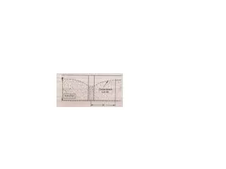
Functional Testing • Voltage Ripple at Various Conditions • Efficiency of the Circuit at Various Conditions • Duty Ratios
Duty Ratio D=|Vout|/(Vin+|Vout|)
Major Problems • Designing a self starting circuit that did not require external voltages caused difficulties due to isolation issues with converter design • Efficiency was low for our converter • This was partially a result of our self starting resistor • Another problem appeared to be in the 12 V FET which was heating excessively and eventually failed. • Failure of the FET in our 12 V supply right before our demo resulted in our 5 V supply acting unstable during our demo.
Conclusions • Design Requirements that need further attention • The 12 V output failure needs to be analyzed and fixed. We believe that the low efficiency of the circuit was possibly due to the problem that caused this failure. • The control circuit needs to be successfully integrated into the gate drive circuitry to improve the Line and Load Regulation
Conclusions • Successfully met design requirements • Single power supply providing DC/DC conversion • Voltage Ripple requirements at various loads • Control Circuit provided desired control function but we were unable to integrate it into the gate drive circuitry