Download
1 / 16
160 likes | 312 Views
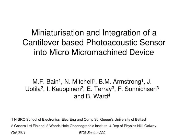
Miniaturisation and Integration of a Cantilever based Photoacoustic Sensor into Micro Micromachined Device. M.F. Bain 1 , N. Mitchell 1 , B.M. Armstrong 1 , J. Uotila 2 , I. Kauppinen 2 , E. Terray 3 , F. Sonnichsen 3 and B. Ward 4.

E N D
Miniaturisation and Integration of a Cantilever based Photoacoustic Sensor into Micro Micromachined Device M.F. Bain1, N. Mitchell1, B.M. Armstrong1, J. Uotila2, I. Kauppinen2, E. Terray3, F. Sonnichsen3 and B. Ward4 1 NISRC School of Electronics, Elec Eng and Comp Sci Queen’s University of Belfast 2 Gasera Ltd Finland, 3 Woods Hole Oceanographic Institute, 4 Dep of Physics NUI Galway ECS Boston 220
Introduction • Cantilevers and Photoacoustic Gas Sensors (PAS) • Motivation for PA cell Miniaturisation • Fabrication of µPAS device • Experimental • Results and Analysis • Further Work ECS Boston 220
Photoacoustic Gas Sensors Highly sensitive Photoacoustic (PA) Gas Sensor Cantilever deflection is measured by laser interferometery focused at the cantilever tip. Sensitivity of 0.001Å ECS Boston 220
PA Cell miniaturisation In conventional spectroscopy sensitivity decreases with dimensions. Photoacoustic spectroscopy response is enhanced as the volume decreases. Using MEMS technology to incorporate the cantilever and gas cavities into one structure. ECS Boston 220
Cavity µPAS Cell: Proposed device Cavity dimensions: ~1mm wide, 12mm long, 250µm deep. Cantilever dimensions: ~ 500µm wide, 500µm length and various thickness. Excitation laser inlet defined 1877nm for CO2 Gas inlet/outlet vias to be etched through the substrate. Quartz window allows deflection measurements using interferometer Quartz Cantilever Gas inlet laser ECS Boston 220
Fabrication: Cavity Substrate (a) The gas inlet/outlet through holes are initially defined with a dry etch (depth ~300µm) (b) the second etch defines the PA cell cavity, approximately 12mm long 1mm wide and ~250µm deep. The gas inlet/outlet meander and the laser inlet are also defined at this stage. (c) plan view of etched cavity substrate. The substrate is still robust enough to be subjected to chemical cleaning. (c) Gas inlet Cavity Laser inlet (b) Gas outlet (a) Silicon Substrate ECS Boston 220
Fabrication: Cavity Substrate ECS Boston 220
Fabrication: Cantilever Substrate length (d) SOI substrate defines the thickness of the cantilever. BOX thickness also important (d) (e) SOI Substrate SOI Substrate Width (e) the cantilever is defined in the SOI substrate prior to bonding. Defining the cantilever length, width and gap size, . ECS Boston 220
(f) the two substrates are bonded such that the cantilever is positioned over the cell cavity using an EV bond aligner. (g) (g) the cavity behind the cantilever is defined and acts as a balance cell. (f) Fabrication: Bonded Structure IR picture of bonded interface. Typical yield on bonded devices is 11/12 or 12/12. ECS Boston 220
Fabrication: Bonded Structure X section shows the gas meander and PA cell. Plan view micrograph of cantilever. Talysurf image of cantilever. ECS Boston 220
Fabrication: Final Structure (g) plan view of device. µPAS devices of thickness 4, 6.5, 10 and 15µm were successfully fabricated. (h) the device is sealed by electrostatic bonding to a quartz substrate. The quartz substrate/window will allow deflection detection by interferometery. Device should be very leak tight. Chips were successfuly bonded to a Si substrate (g) Gas inlet Cantilever Laser inlet Cavity Gas outlet (h) ECS Boston 220
Test jig for the µPAS allows N2 pressurization of device through the gas vias and cavity. µPAS device mounted and clamped to prevent leaks. N2 pressure controlled and monitored. Measurement of cantilever shape using white light interferometery. Fringes show the cantilever is inplane with the SOI surface. Fringes show the cantilever is deflected occurs due to N2 pressure Pressure Sensor Vent ATM µPAS Test jig N2 Regulator Experimental ECS Boston 220
µPAS devices of thickness 4, 6.5, 10 and 15µm were successfully fabricated. At rest deflection was measured. (L-0.5, W-0.5mm) Results and Analysis The µPAS devices were subjected to a range of pressures and deflection was measured. Deflection, calculations ECS Boston 220
A SOI substrate (4µm thick) was bonded to a cavity substrate. This produced a diaphragm structure over the PA cell. The cantilever substrate 4µm is also thick, allowing a direct comparison between the diaphragm and cantilever structures over the same pressure range. 0.25 2.5 4.5 Results and Analysis The cantilever is an order of magnitude more sensitive than the diaphragm ECS Boston 220
Future work • Insertion of laser to excite specific gases and measure using interferometer • Reference cells fill with specific gas at the bonding level • Multiple cantilevers for reference and increased sensitivity ECS Boston 220
Acknowledgements Financial support of the National Science Foundation (USA) Science Foundation of Ireland Dept of Education and Learning (NI) Questions? ECS Boston 220