Download
1 / 67

E N D
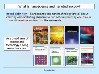
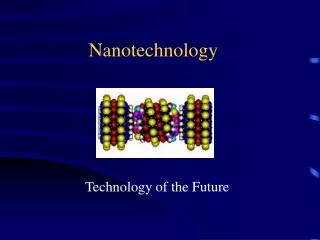
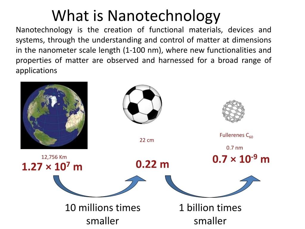
What is Nanotechnology Nanotechnology is the creation of functional materials, devices and systems, through the understanding and control of matter at dimensions in the nanometer scale length (1-100 nm), where new functionalities and properties of matter are observed and harnessed for a broad range of applications Fullerenes C60 22 cm 0.7 nm 0.7 × 10⁻⁹ m 12,756 Km 0.22 m 1.27 × 10⁷ m 10 millions times smaller 1 billion times smaller
History of Nanotechnology • ~ 2000 Years Ago – Sulfide nanocrystals used by Greeks and Romans to dye hair • ~ 1000 Years Ago (Middle Ages) – Gold nanoparticles of different sizes used to produce different colors in stained glass windows • 1959 – “There is plenty of room at the bottom” by R. Feynman • 1974 – “Nanotechnology” - Taniguchi uses the term nanotechnology for the first time • 1981 – IBM develops Scanning Tunneling Microscope • 1985 – “Buckyball” - Scientists at Rice University and University of Sussex discover C60
Lycurgus Cup Lycurgus Cup is made of glass. Roman ~400 AD, Myth of King Lycurgus Appears green in reflected light and red in transmitted light http://www.thebritishmuseum.ac.uk/science/lycurguscup/sr-lycugus-p1.html
The Institute of Nanotechnology http://www.nano.org.uk/ • Technology re-discovered in the 1600s and used for colored stained glass windows
When Nanotechnology started ? • The concepts that seeded nanotechnology were first discussed in 1959 by renowned physicist Richard Feynman in his talk There's Plenty of Room at the Bottom, in which he described the possibility of synthesis via direct manipulation of atoms. • The term "nano-technology" was first used by Norio Taniguchi in 1974, though it was not widely known. • The invention of the scanning tunneling microscope in 1981 provided unprecedented visualization of individual atoms and bonds, and was successfully used to manipulate individual atoms in 1989 • Fullerenes were discovered in 1985 by Harry Kroto, Richard Smalley, and Robert Curl, who together won the 1996 Nobel Prize in Chemistry • The microscope's developers Gerd Binnig and Heinrich Rohrer at IBM Zurich Research Laboratory received a Nobel Prize in Physics in 1986. By the mid-2000s new and serious scientific attention to Nanotechnology
1986 – “Engines of Creation” - First book on nanotechnology by K. Eric Drexler. Atomic Force Microscope invented by Binnig, Quate and Gerbe • 1989 – IBM logo made with individual atoms • 1991 – Carbon nanotube discovered by SumioIijimaJapanese electron microscopist , who was studying the material deposited on the cathode during the arc-evaporation synthesis of fullerenes. He found that the central core of the cathodic deposit contained a variety of closed graphitic structures including nanoparticles and nanotubes, of a type which had never previously been observed • 1999 – “Nanomedicine” – 1st nanomedicine book by R. Freitas • 2000 – “National Nanotechnology Initiative” launched
Nanoscale Size EffectChemical - Physical - Mechanical - Optical Reduced density Enhanced diffusivity Increased specific heat Reduced elastic modulus Higher electrical resistivity Lower thermal conductivity Increased strength/hardness Improved ductility/toughness Superior soft magnetic properties Higher thermal expansion coefficient
Introduction to ‘NANO’ Exist as Crystallites three dimension Layers two dimension Filaments one dimension Clusters zero dimension Nano size range 1-100nm Demand for size range 20nm has become more crucial Nanomaterials are single-phase or multiphase poly- crystals with a typical crystal size of 1 to 100 nm in at least one dimension.
Nanomaterials - most fascinating materials of today Properties: Bulk gold melts at 1064 °C, but particles in the 5 nm size range melts at about 830 °C. Electronic band of a crystal is gradually quantised as the size is reduced, resulting in an increase in the band-gap energy. Cobalt normally has a hexagonal lattice arrangement, but this is transformed to non-hexagonal for Cobalt particles smaller than about 20 nm.
Can we go below nano ? Obviously when the size of the crystallites shrinks beyond the ‘nano’ size, many atoms become part of the crystallites surface rather than being fully bonded ‘bulk’ atoms. Surface atoms are distinguished by their reduced coordination to the crystal backbone. Hence they are more prone to react with surrounding ambient or they exhibit other unusual physical phenomena. R. Tenne, Angew Chem. Int Ed. 42(2003)5124
Why Nanotechnology • we are interested in the nano scale materials because they exhibit different physical and chemical properties over bulk materials • Materials having very small sizes have unique properties • The size of the particles controls the colors that are emitted when the particles are exposed to UV light • Only certain chemical compositions will have this property (i.e. this behavior is not generic to all nanoparticles) • Materials with small sizes can be packed like • Integrated circuits: Millions of electrical components (resistors, transistors) per square inch
What is nanomaterial ? • Is defined as any material that has unique or novel properties, due to the nanoscale ( nanometre- scale) structuring. • They are subdivided into One-dimensional nanomaterials, Two-dimensional nanomaterials, Zero-dimensional nanomaterials 3 D Bulk 0D 1D 2D T Pradep et al “ Nano the essentials”
3D 2D 1D 0D • If a bulk metal is made thinner and thinner, until the electrons can move only in two dimensions (instead of 3D), then it is “2D quantum confinement.” • Next level is ‘quantum wire • Ultimately ‘quantum dot’ Source: Nanoscale Materials in Chemistry, Wiley, 2001
Size effects The properties of a material depend on the type of motion of its electrons can execute, which depends on the space available for them. Thus, the properties of a material are characterized by a specific “length scale”, usually on the nm dimension. If the physical size of the material is reduced below this length scale, its properties change and become sensitive to size and shape. Exhibition of different color is due to different mode of interaction of light with the gold involving surface plasmons.
0D Nanoparticles, quantum dots 1D Nano wires 200 nm 500 nm 2D 1µm Nanowalls, nanoplates, thin films 5µm 2µm
Approaches to Nano Materials (growth methods) Bottom-up or top-down • Bottom-up approaches seek to have smaller atoms and molecules to build more complex assemblies, while top-down approaches seek to create nano scale devices from bulk • The top-down approach often uses the traditional workshop or micro fabrication methods where externally controlled tools are used to cut, mill, and shape materials into the desired shape and order.
How to prepare nanostructures Bottom up Nano particles Evaporation, CVD, MOCVD, ALD, template assisted. Liquid phase self assembly and electro deposition Clusters Atoms
Bottom Up approach Nanoparticles Nanotubes Nanowires Vapor phase growth
Top down How to prepare nanostructures Bulk Powder Nano particles Lithography, etching, removal
Different techniques to grow nanostructures Nanostructures growth Vapor phase growth Solution based growth Physical vapor deposition (PVD) Chemical vapor deposition (CVD) Hydro thermal Sol Gel Electron beam and Thermal evaporation Metal Organic CVD Electro chemical deposition Pulsed laser deposition (PLD) Plasma enhanced CVD Sputtering Atomic layer deposition (ALD) Activated reactive evaporation 25 Mehta et al. Appl. Phys. Lett. 79 3176 (2001)
Synthesis of NanomaterialsSeveral synthetic routes are practiced that either break larger particles to nanosize or employ nucleation and growth. But control at the desired stage of the process is difficult in many of them. Sol Gel Co-precipitation Hydrothermal Chemist route (building up process)Chemical Vapour Deposition (CVD) Inverse micelle method Solution combustion synthesis (SCS) Spark Erosion Inert Gas Condensation Laser Ablation Physicist route (breaking down process)Mechanical Attrition Plasma pyrolysis Sputtering
Synthesis of Nanomaterials Several synthetic routes are practiced that either break larger particles to nanosize or employ nucleation and growth. But control at the desired stage of the process is difficult in many of them Chemist routePhysicist route (building - up process) (breaking - down process) Sol GelSpark Erosion Co-precipitationInert Gas Condensation HydrothermalLaser Ablation Inverse micelle method Mechanical Attrition Chemical Vapour Deposition Plasma pyrolysis (CVD) Sputtering Combustion Synthesis (Integrated approach)
Applications of Nanocrystalline Oxide Materials ABRASIVES: Al2O3, CeO2, Fe2O3 CATALYSIS: TiO2, CeO2, Fe2O3, M/ Al2O3, M/CeO2, Pt/TiO2 COSMETICS: TiO2, ZnO ELECTRONICS: BaTiO3, ZnO, Al2O3, PZT MAGNETICS: - Fe2O3, BaFe12O19, MFe2O4 PIGMENTS AND COATINGS: TiO2, Fe2O3, Cr2O3, ZnO PHOSPHORS: Eu3+/Y2O3(Red), Eu2+, Tb/Ba- Hexaaluminate STRUCTURAL CERAMICS: Al2O3, ZrO2, ZTA, Mullite, Cordierite, Tialite FUEL CELLS: Solid Oxide Fuel Cell Materials YSZ(Y2O3-ZrO2) Electrolyte Ni/YSZ Ln(Sr)MO3, M=Mn, Cr WATER PURIFICATION: MgO, ZnO, CaO and others
Redox Mixtures - Solution Combustion Process • It uses an aqueous solution containing stoichiometric amounts of oxidizer and a fuel. • The fuels used are Urea (U), glycine (GLY) carbohydrazide (CH), oxalyldihydrazide (ODH), tetraformaltrisazine (TFTA) hexamethylenetetraamine (HMT) and other derivatives of hydrazine. • The redox mixture when heated rapidly at ~500C froths, fumes and ignites to give the product in just few minutes. • This process is an exothermic redox reaction that is self-propagating & gas-producing once initiated at low temperatures. • The products are very fine, voluminous, homogenous and of high purity.
Nanoparticles • Nanoparticles are typically solid structures of inorganic elements of the size ~1-100 nm • Magnetic • Optical • Melting points • Specific heats • Surface reactivity • Monodisperse (±15%) • Stable distribution • Interaction between the two components • Structure-property relationships • Inclusion of functionalities
Quantum well • It is a two dimensional system • The electron can move in two directions and restricted in one direction. • Quantum Wire • It is a one-dimensional system • The electron can move in one direction and restricted in two directions. • Quantum dot • It is a zero dimensional system • The electron movement was restricted in entire three dimensions
In quantum dot all the three dimensions are reduced to zero Quantum dot
Nanomaterials have the structural features in between of those of atoms and the bulk materials. While most microstructured materials have similar properties to the corresponding bulk materials, the properties of materials with nanometer dimensions are significantly different from those of atoms and bulks materials. This is mainly due to the nanometer size of the materials which render them: (i) large fraction of surface atoms; (ii) high surface energy; (iii) spatial confinement; (iv) reduced imperfections, which do not exist in the corresponding bulk materials. Due to their small dimensions, nanomaterials have extremely large surface area to volume ratio, which makes a large to be the surface or interfacial atoms, resulting in more “surface” dependent material properties. Physical properties 1. Large fraction of surface atoms. 2. Large surface energy. 3. Spatial confinement. 4. Reduced imperfections. 5. Lower melting point. 6. Lower phase transition temperature. 7. Reduced lattice constants due to a huge fraction of surface atoms
Melting Point The melting point decreases dramatically as the particle size gets below 5 nm Source: Nanoscale Materials in Chemistry, Wiley, 2001
Band gap The band gap is increases with reducing the size of the particles
Surface Area The total surface area (or) the number of surface atom increases with reducing size of the particles
Nanostructure Properties Surface to Volume Ratio • Surface and interface properties (e.g. adhesive and frictional forces) become critical as materials become smaller • High surface area materials have applications in: energy storage, catalysis, battery/capacitor elements, gas separation and filtering, biochemical separations, etc.
Size-Dependent Properties of semiconductor and magnetic materials • For semiconductors such as ZnO, CdS, and Si, the bandgap changes with size - Bandgap is the energy needed to promote an electron from the valence band to the conduction band - When the bandgaps lie in the visible spectrum, changing bandgap with size means a change in color • For magnetic materials such as Fe, Co, Ni, Fe3O4, etc., magnetic properties are size dependent - The ‘coercive force’ (or magnetic memory) needed to reverse an internal magnetic field within the particle is size dependent - The strength of a particle’s internal magnetic field can be size dependent
Synthesis of Nanomaterials Several synthetic routes are practiced that either break larger particles to nanosize or employ nucleation and growth. But control at the desired stage of the process is difficult in many of them Chemist routePhysicist route (building - up process) (breaking - down process) Sol GelSpark Erosion Co-precipitationInert Gas Condensation HydrothermalLaser Ablation Inverse micelle method Mechanical Attrition Chemical Vapour Deposition Plasma pyrolysis (CVD) Sputtering Combustion Synthesis (Integrated approach)
Combustion or Fire Synthesis of Oxide Materials * Two methods: Redox compounds: M-hydrazine carboxylate precursors Ignition temperature - 120 - 3000C Redox mixtures: Metal nitrates / perchlorates (Oxidizer) Urea / hydrazides (Fuels) Ignition temperature - 350 - 5000C *K.C.Patil, et.al, - total number of citations 2,125 (2003 – 2007) K.C.Patil, S.T.Aruna and S.Ekambaram, ‘Combustion Synthesis’, “Current Opinion in Solid State and Matter’. Sci.”, 2 (1997) 158-165. (cited 71 times) K.C.Patil, S.T.Aruna and T.Mimani, ‘Combustion Synthesis: An update’, “Current Opinion in Solid State and Mater. Sci.”, 6 (2002) 507-512. (cited 55 times)
Redox Mixtures - Solution Combustion Process • It uses an aqueous solution containing stoichiometric amounts of oxidizer and a fuel. • The fuels used are Urea (U), glycine (GLY) carbohydrazide (CH), oxalyldihydrazide (ODH), tetraformaltrisazine (TFTA) hexamethylenetetraamine (HMT) and other derivatives of hydrazine. • The redox mixture when heated rapidly at ~500C froths, fumes and ignites to give the product in just few minutes. • This process is an exothermic redox reaction that is self-propagating & gas-producing once initiated at low temperatures. • The products are very fine, voluminous, homogenous and of high purity.
Combustion method: • low temperature, time saving, energy efficient, self propagating method, involving spontaneous exothermic redox reaction between metal nitrate and organic fuel, used to prepare nanomaterials. • Principle: The method is based on the utilization of heat energy produced during the exothermic spontaneous redox reaction between an oxidizer (metal nitrate) and a reducing agent (organic fuel). The oxidizer can be of any metal nitrates and reducing agents may be organic fuels, such as glycine, oxalic acid, urea, hexamine, sugar, EDTA, Detrose etc. • 500 ºC CºC • Metal nitrate + Fuel nano Metal oxide + Gases
most important advantages of SCS process • It is an easy and fast process that uses relatively simple equipment. • High-purity products can be easily prepared by using this method. • Composition, structure, homogeneity, size and stoichiometry of the products can be controlled. • High exothermicity of the metal nitrate–fuel reaction permits incorporation of desired quantity • of dopants in the various hosts of industrially useful phosphors. • This is the cheap method as compared to conventional solid state method.
amount of fuel For the calculation of valency of fuel and metal nitrate, the valency to be considered for the elements such as of N, O, H, C, and Mn+ are 0, -2, +1, +4 and +n respectively.