Download
1 / 16
160 likes | 288 Views
SIZE DEPENDENT TRANSPORT IN DOPED NANOWIRES. Qin Zhang Anubhav Khandelwal Jeffrey Bean December 13, 2004. OUTLINE. Introduction and Motivation Bandgap variation in 1D wires Impurity binding energy Carrier concentration in 1D wires Roughness scattering limited momentum relaxation time

E N D
SIZE DEPENDENT TRANSPORT IN DOPED NANOWIRES Qin Zhang Anubhav Khandelwal Jeffrey Bean December 13, 2004 Advanced Semiconductor Physics ~ Dr. Jena University of Notre Dame Department of Electrical Engineering
OUTLINE • Introduction and Motivation • Bandgap variation in 1D wires • Impurity binding energy • Carrier concentration in 1D wires • Roughness scattering limited momentum relaxation time • Mobility in nanowires • Conclusion Advanced Semiconductor Physics ~ Dr. Jena University of Notre Dame Department of Electrical Engineering
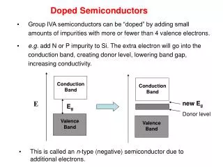
Introduction and Motivation • In low dimensional structures, such as nanowires, quantum effects change electrical properties: • electronic band gap • impurity binding energy • carrier concentration • carrier mobility • Doping in nanowires • Mobility in nanowires Advanced Semiconductor Physics ~ Dr. Jena University of Notre Dame Department of Electrical Engineering
Bandgap Variation • For a quantum wire, confinement energy is given by: in nm Advanced Semiconductor Physics ~ Dr. Jena University of Notre Dame Department of Electrical Engineering
Effective Mass Approximation • Advantages • Simplest • Dimensional Effect • Surface Effect • Limits • effective mass from bulk semiconductors is not good assumption when d is very small • parabolic band structure is not a good approximation when Eg is small Advanced Semiconductor Physics ~ Dr. Jena University of Notre Dame Department of Electrical Engineering
Impurity Binding Energy • The binding energy was calculated using the expression1: where: • We have considered the cases when the impurity is located on the axis, at the midpoint between the axis and edge, and on the edge(t0=0, ½, 1 respectively) of the wire for different values of d 1. J. W. Brown and H. N. Spector, J. Appl. Phys 59, 1179 (1986) Advanced Semiconductor Physics ~ Dr. Jena University of Notre Dame Department of Electrical Engineering
We have determined the hydrogenic binding energies (in meV) as a function of wire radius (in nm) for CdSe, GaAs, and Si using parameters as listed below. a0*(nm) me*/m0 ε/ε0 R0*(meV) 11.7 0.63 978 Si 0.98 12.9 10.78 52 GaAs 0.063 10.2 4.13 17 CdSe 0.13 Binding Energy Binding energy vs. Wire radius for CdSe Binding energy vs. Wire radius for Si Binding energy vs. Wire radius for GaAs Advanced Semiconductor Physics ~ Dr. Jena University of Notre Dame Department of Electrical Engineering
Carrier Concentration • For the 1-D case, the total electron concentration in the conduction band is: • Where: gc1D(E) is the density of states (DOS) for 1-D f(E) is the Fermi distribution function. • Under non-degenerate conditions, where: Advanced Semiconductor Physics ~ Dr. Jena University of Notre Dame Department of Electrical Engineering
Carrier Concentration • Using the charge-neutral relationship for n-type material: • Since Eb depends on the position of impurities, n needs to be averaged: • This equation is solved numerically. Here we assume the doping is uniform along the axis of the nanowires. Advanced Semiconductor Physics ~ Dr. Jena University of Notre Dame Department of Electrical Engineering
n as T and Nd n as T and d n as d and Nd CdSe Carrier Concentrations… Electron concentration in the conduction band of CdSe: n vs. d with T=300K and different doping densites Electron concentration in the conduction band of CdSe: n vs. Temperature with constant radius and different doping densites Electron concentration in the conduction band of CdSe: n vs. temperature for constant doping density and different wire radii Advanced Semiconductor Physics ~ Dr. Jena University of Notre Dame Department of Electrical Engineering
Carrier Concentration • Electron concentration for CdSe, GaAs, and Si vs. wire radius with doping density of 5*105 cm-1 at 300K Advanced Semiconductor Physics ~ Dr. Jena University of Notre Dame Department of Electrical Engineering
Roughness Scattering Limited Momentum Relaxation Time • For a quantum wire, confinement energy is given by: • For the ground state wave function: • Roughness potential V(z) is given by: • Roughness S(z) is assumed to be Gaussian and is expressed as where Δ is the maximum height and Λ is the full width half max of the roughness. Advanced Semiconductor Physics ~ Dr. Jena University of Notre Dame Department of Electrical Engineering
Roughness Scattering Limited Momentum Relaxation Time • Momentum relaxation time is given by: • where: • total carrier density N1V = nL, n is carrier density (cm-1), L is the wire length, θ is the angle between the initial and final wavevectors k and k’ • Calculating the matrix elements: where: Advanced Semiconductor Physics ~ Dr. Jena University of Notre Dame Department of Electrical Engineering
Roughness Scattering Limited Momentum Relaxation Time • Momentum relaxation time is calculated as: • where k10d=2.405 (first root of J1(k10d)), which gives the final expression for tm-1 • The momentum relaxation time is given by: • The mobility is then given by: where: kF is the Fermi wave vector given by pn/2 Advanced Semiconductor Physics ~ Dr. Jena University of Notre Dame Department of Electrical Engineering
1: d=20nm 2: d=10nm 3: d=5nm Roughness Scattering Limited Momentum Relaxation Time mobility µ as a function of n for different X(=Λ) mobility µ as a function of d for different X(=Λ) mobility µ as a function of X(=Λ) for two values of n equal to 104 cm-1 and 105 cm-1 Advanced Semiconductor Physics ~ Dr. Jena University of Notre Dame Department of Electrical Engineering
Conclusions • Hydrogenic impurity binding energy in a quantum wire: • Decreases as wire radius increases • Maximum when impurity is on the wire axis • The electron carrier density: • Increases when wire radius, temperature, and doping density increase • Incomplete ionization at room temperature • Percentage of ionization decreases as doping density increases and temperature decreases • surface roughness limited momentum relaxation time: • Mobility varies as a function of d6 • Mobility first decreases, then increases as roughness variation Λ is increased, and reaches a maximum at the Fermi wavelength • Questions??? Advanced Semiconductor Physics ~ Dr. Jena University of Notre Dame Department of Electrical Engineering