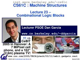
Download
1 / 24
240 likes | 320 Views
CS 61C: Great Ideas in Computer Architecture (Machine Structures) Lecture 28: Single-Cycle CPU Datapath Control Part 1. Instructor: Senior Lecturer SOE Dan Garcia http:// inst.eecs.Berkeley.edu /~cs61c/sp13. Review. CPU design involves Datapath , Control 5 Stages for MIPS Instructions

E N D
CS 61C: Great Ideas in Computer Architecture (Machine Structures)Lecture 28: Single-Cycle CPUDatapath Control Part 1 Instructor: Senior Lecturer SOE Dan Garcia http://inst.eecs.Berkeley.edu/~cs61c/sp13
Review • CPU design involves Datapath, Control • 5 Stages for MIPS Instructions • Instruction Fetch • Instruction Decode & Register Read • ALU (Execute) • Memory • Register Write • Datapath timing: single long clock cycle or one short clock cycle per stage
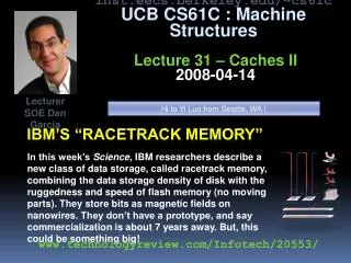
www.technologyreview.com/news/512776/microchip-adapts-to-severe-damage/www.technologyreview.com/news/512776/microchip-adapts-to-severe-damage/ Technology In the News Microchip works after damage by routing around it Researchers at CalTech have developed an integrated circuit (IC) that can continue to perform in the face of structural damage. “It doesn’t physically repair flaws, it uses a second processor to come up with new ways to perform a task in spite of the damage. It can also be programmed to prioritize energy savings or speed”. In some sense, like the Internet, that can “route around” trouble spots.
rd instruction memory PC registers rs Data memory ALU rt +4 imm opcode, funct Controller Datapathand Control • Datapath based on data transfers required to perform instructions • Controller causes the right transfers to happen
2. Decode/ Register Read 5. Reg. Write 1. Instruction Fetch 4. Memory 3. Execute CPU Clocking (1/2) • For each instruction, how do we control the flow of information though the datapath? • Single Cycle CPU: All stages of an instruction completed within one long clock cycle • Clock cycle sufficiently long to allow each instruction to complete all stages without interruption within one cycle
2. Decode/ Register Read 1. Instruction Fetch 4. Memory 3. Execute 5. Register Write CPU Clocking (2/2) • Alternative multiple-cycle CPU: only one stage of instruction per clock cycle • Clock is made as long as the slowest stage • Several significant advantages over single cycle execution: Unused stages in a particular instruction can be skipped OR instructions can be pipelined (overlapped)
Agenda • Stages of the Datapath • Datapath Instruction Walkthroughs • DatapathDesign
Five Components of a Computer Keyboard, Mouse Computer Devices Memory (passive) (where programs, data live when running) Processor Disk(where programs, data live when not running) Input Control Output Datapath Display, Printer
Processor Design: 5 steps Step 1: Analyze instruction set to determinedatapath requirements • Meaning of each instruction is given by register transfers • Datapath must include storage element for ISA registers • Datapath must support each register transfer Step 2: Select set of datapath components & establish clock methodology Step 3: Assemble datapath components that meet the requirements Step 4: Analyze implementation of each instruction to determine setting of control points that realizes the register transfer Step 5: Assemble the control logic
31 26 21 16 11 6 0 op rs rt rd shamt funct 6 bits 5 bits 5 bits 5 bits 5 bits 6 bits 31 26 21 16 0 address/immediate op rs rt 6 bits 5 bits 5 bits 16 bits 31 26 0 op target address 6 bits 26 bits The MIPS Instruction Formats • All MIPS instructions are 32 bits long. 3 formats: • R-type • I-type • J-type • The different fields are: • op: operation (“opcode”) of the instruction • rs, rt, rd: the source and destination register specifiers • shamt: shift amount • funct: selects the variant of the operation in the “op” field • address / immediate: address offset or immediate value • target address: target address of jump instruction
31 26 21 16 11 6 0 op rs rt rd shamt funct 6 bits 5 bits 5 bits 5 bits 5 bits 6 bits 31 26 21 16 0 op rs rt immediate 6 bits 5 bits 5 bits 16 bits 31 26 21 16 0 op rs rt immediate 6 bits 5 bits 5 bits 16 bits 31 26 21 16 0 op rs rt immediate 6 bits 5 bits 5 bits 16 bits The MIPS-lite Subset • ADDU and SUBU • addu rd,rs,rt • subu rd,rs,rt • OR Immediate: • ori rt,rs,imm16 • LOAD and STORE Word • lw rt,rs,imm16 • sw rt,rs,imm16 • BRANCH: • beq rs,rt,imm16
Register Transfer Language (RTL) RTL gives the meaning of the instructions All start by fetching the instruction {op , rs , rt , rd , shamt , funct} MEM[ PC ] {op , rs , rt , Imm16} MEM[ PC ] InstRegister Transfers ADDU R[rd] R[rs] + R[rt]; PC PC + 4 SUBU R[rd] R[rs] – R[rt]; PC PC + 4 ORI R[rt] R[rs] | zero_ext(Imm16); PC PC + 4 LOAD R[rt] MEM[ R[rs] + sign_ext(Imm16)]; PC PC + 4 STORE MEM[ R[rs] + sign_ext(Imm16) ] R[rt]; PC PC + 4 BEQ if ( R[rs] == R[rt] ) then PC PC + 4 + (sign_ext(Imm16) || 00) else PC PC + 4
Step 1: Requirements of the Instruction Set • Memory (MEM) • Instructions & data (will use one for each) • Registers (R: 32 x 32) • Read RS • Read RT • Write RT or RD • PC • Extender (sign/zero extend) • Add/Sub/OR unit for operation on register(s) or extended immediate • Add 4 (+ maybe extended immediate) to PC • Compare registers?
Adder ALU Step 2: Components of the Datapath CarryIn A • Combinational Elements • Storage Elements + Clocking Methodology • Building Blocks 32 Sum 32 B CarryOut 32 Select A 32 MUX Y 32 B 32 OP ALU Multiplexer A Adder 32 Result 32 B 32
ALU Needs for MIPS-lite + Rest of MIPS • Addition, subtraction, logical OR, ==: ADDU R[rd] = R[rs] + R[rt]; ... SUBU R[rd] = R[rs] – R[rt]; ... ORI R[rt] = R[rs] | zero_ext(Imm16)... BEQ if ( R[rs] == R[rt] )... • Test to see if output == 0 for any ALU operation gives == test. How? • P&H also adds AND, Set Less Than (1 if A < B, 0 otherwise) • ALU follows Chapter 5
Storage Element: Idealized Memory Write Enable Address • Memory (idealized) • One input bus: Data In • One output bus: Data Out • Memory word is found by: • Address selects the word to put on Data Out • Write Enable = 1: address selects the memoryword to be written via the Data In bus • Clock input (CLK) • CLK input is a factor ONLY during write operation • During read operation, behaves as a combinational logic block: Address valid Data Out valid after “access time” Data In DataOut 32 32 Clk
Write Enable Data In Data Out N N clk Storage Element: Register (Building Block) • Similar to D Flip Flop except • N-bit input and output • Write Enable input • Write Enable: • Negated (or deasserted) (0): Data Out will not change • Asserted (1): Data Out will become Data In on positive edge of clock
Storage Element: Register File RW RA RB Write Enable 5 5 5 • Register File consists of 32 registers: • Two 32-bit output busses: busA and busB • One 32-bit input bus: busW • Register is selected by: • RA (number) selects the register to put on busA (data) • RB (number) selects the register to put on busB (data) • RW (number) selects the register to be writtenvia busW (data) when Write Enable is 1 • Clock input (clk) • Clk input is a factor ONLY during write operation • During read operation, behaves as a combinational logic block: • RA or RB valid busA or busB valid after “access time.” busA busW 32 32 x 32-bit Registers 32 busB Clk 32
Next Address Logic Address Instruction Memory Step 3a: Instruction Fetch Unit • Register Transfer Requirements Datapath Assembly • Instruction Fetch • Read Operands and Execute Operation • Common RTL operations • Fetch the Instruction: mem[PC] • Update the program counter: • Sequential Code: PC PC + 4 • Branch and Jump: PC “something else” clk PC Instruction Word 32
Step 3b: Add & Subtract • R[rd] = R[rs] op R[rt] (addurd,rs,rt) • Ra, Rb, and Rw come from instruction’s Rs, Rt, and Rd fields • ALUctr andRegWr: control logic after decoding the instruction • … Already defined the register file & ALU 31 26 21 16 11 6 0 op rs rt rd shamt funct 6 bits 5 bits 5 bits 5 bits 5 bits 6 bits Rd Rs Rt ALUctr RegWr 5 5 5 busA Rw Ra Rb busW 32 Result 32 x 32-bit Registers ALU 32 32 busB clk 32
Clocking Methodology Clk • Storage elements clocked by same edge • Flip-flops (FFs) and combinational logic have some delays • Gates: delay from input change to output change • Signals at FF D input must be stable before active clock edge to allow signal to travel within the FF (set-up time), and we have the usual clock-to-Q delay • “Critical path” (longest path through logic) determines length of clock period . . . . . . . . . . . .
ALU Register-Register Timing: One Complete Cycle Clk Old Value New Value PC Instruction Memory Access Time Rs, Rt, Rd, Op, Func Old Value New Value Delay through Control Logic ALUctr Old Value New Value RegWr Old Value New Value Register File Access Time busA, B Old Value New Value ALU Delay busW Old Value New Value ALUctr RegWr Rd Rs Rt 5 5 5 Register Write Occurs Here busA 32 Rw Ra Rb busW 32 RegFile busB 32 clk
Inst Memory Adr Adder Adder Mux 1 0 = 00 ALU 0 PC 0 WrEn Adr 1 1 Extender Data Memory PC Ext Putting it All Together:A Single Cycle Datapath Instruction<31:0> <0:15> <21:25> <16:20> <11:15> Rs Rt Rd Imm16 RegDst nPC_sel MemtoReg ALUctr Rd Rt Equal MemWr RegWr Rs Rt 4 5 5 5 busA 32 Rw Ra Rb busW 32 RegFile busB 32 32 clk 32 clk imm16 Data In 16 32 clk imm16 ExtOp ALUSrc
Processor Design: 3 of 5 steps Step 1: Analyze instruction set to determinedatapath requirements • Meaning of each instruction is given by register transfers • Datapath must include storage element for ISA registers • Datapath must support each register transfer Step 2: Select set of datapath components & establish clock methodology Step 3: Assemble datapath components that meet the requirements Step 4: Analyze implementation of each instruction to determine setting of control points that realizes the register transfer Step 5: Assemble the control logic