Download
1 / 27
280 likes | 287 Views
EE105 - Spring 2007 Microelectronic Devices and Circuits. Lecture 2 Semiconductor Basics. Periodic Table of Elements. (1s) 2. (2s) 2. (2p) 6. Electronic Properties of Silicon. Silicon is in Group IV (atomic number 14) Atom electronic structure: 1s 2 2s 2 2p 6 3s 2 3p 2

E N D
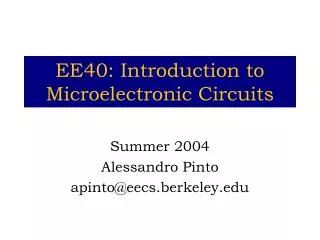
EE105 - Spring 2007Microelectronic Devices and Circuits Lecture 2 Semiconductor Basics
(1s)2 (2s)2 (2p)6 Electronic Properties of Silicon • Silicon is in Group IV (atomic number 14) • Atom electronic structure: 1s22s22p63s23p2 • Crystal electronic structure: 1s22s22p63(sp)4 • Diamond lattice, with 0.235 nm bond length • Very poor conductor at room temperature: why? (3sp)4 Hybridized State
The Diamond Structure 3sp Tetrahedral Bond
. . . E3 Allowed Energy Levels E2 Energy Forbidden Band Gap E1 Atomic Spacing Lattice Constant States of an Atom • Quantum Mechanics: The allowed energy levels for an atom are discrete (2 electrons with opposite spin can occupy a state) • When atoms are brought into close contact, these energy levels split • If there are a large number of atoms, the discrete energy levels form a “continuous” band
Silicon • Si has four valence electrons. Therefore, it can form covalent bonds with four of its neighbors. • When temperature goes up, electrons in the covalent bond can become free.
Electron-Hole Pair Interaction • With free electrons breaking off covalent bonds, holes are generated. • Holes can be filled by absorbing other free electrons, so effectively there is a flow of charge carriers.
Free Electron Density as a Function of Temperature • Eg, or bandgap energy, determines how much effort is needed to break off an electron from its covalent bond. • There exists an exponential relationship between the free-electron density and bandgap energy.
N Type Doping • If Si is doped with group-V elements such as phosphorous (P) or arsenic (As), then it has more electrons and becomes N type (electron). • Group-V impurities are called Donors
P Type Doping • If Si is doped with group-III elements such as boron (B), then it has more holes and becomes P type. • Group-III impurities are called Acceptors
Thermal Equilibrium (Pure Si) • Balance between generation and recombination determines no = po • Strong function of temperature: T = 300 K
Mass Action Law • The product of electron and hole densities is ALWAYS equal to the square of intrinsic electron density, regardless of doping levels
Compensated Doping • Si is doped with both donor and acceptor atoms: • More donors than acceptors: Nd > Na N type • More acceptors than donors: Na > Nd P type
First Charge Transportation Mechanism: Drift Mobility • The process in which charge particles move because of an electric field is called drift. • Charge particles will move at a velocity that is proportional to the electric field.
Mobility vs. Doping in Silicon at 300K • Typical values
Current Flow: General Case • Electric current is calculated as the amount of charge in v meters that passes thru a cross-section if the charge travel with a velocity of v m/s.
Current Flow: Drift • Since velocity is equal to E, drift characteristic is obtained by substituting v with E in the general current equation. • The total current density consists of both electrons and holes.
Velocity Saturation • A topic treated in more advanced courses is velocity saturation. • In reality, velocity does not increase linearly with electric field. It will eventually saturate to a critical value.
Second Charge Transportation Mechanism: Diffusion • Charge particles move from a region of high concentration to a region of low concentration.
Current Flow: Diffusion Diffusion Coefficient • Diffusion current is proportional to the gradient of charge (dn/dx) along the direction of current flow. • Total diffusion current density consists of both electrons and holes.
Example: Linear vs. Nonlinear Charge Density Profile • Linear charge density profile means constant diffusion current, whereas nonlinear charge density profile means varying diffusion current.
p Einstein's Relation • While the underlying physics behind drift and diffusion currents are totally different, Einstein’s relation provides a link between the two.
Sheet Resistance (Rs) • IC resistors have a specified thickness – not under the control of the circuit designer • Eliminate thickness, t, by absorbing it into a new parameter: the sheet resistance (Rs) “Number of Squares”
Using Sheet Resistance (Rs) • Ion-implanted (or “diffused”) IC resistor
Idealizations • Why does current density Jn “turn”? • What is the thickness of the resistor? • What is the effect of the contact regions?